Self-growing noble metal plasma element nano-structure and application thereof to increase of light absorption of GaInP-based solar cell
A technology of solar cells and nanostructures, applied in circuits, electrical components, photovoltaic power generation, etc., can solve the problems of incomplete etching of aluminum films, high production costs, and complicated preparation processes, so as to avoid the pattern preparation process and improve light absorption Efficiency, the effect of simple preparation process
- Summary
- Abstract
- Description
- Claims
- Application Information
AI Technical Summary
Problems solved by technology
Method used
Image
Examples
Embodiment 1
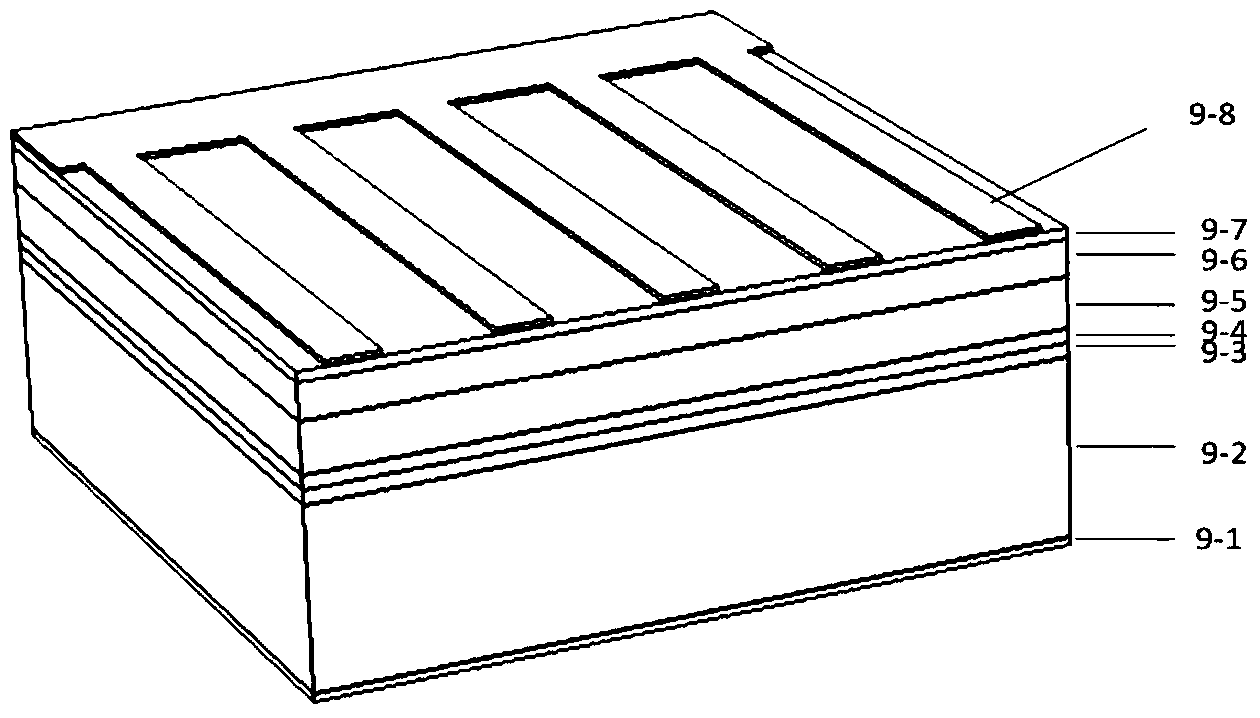
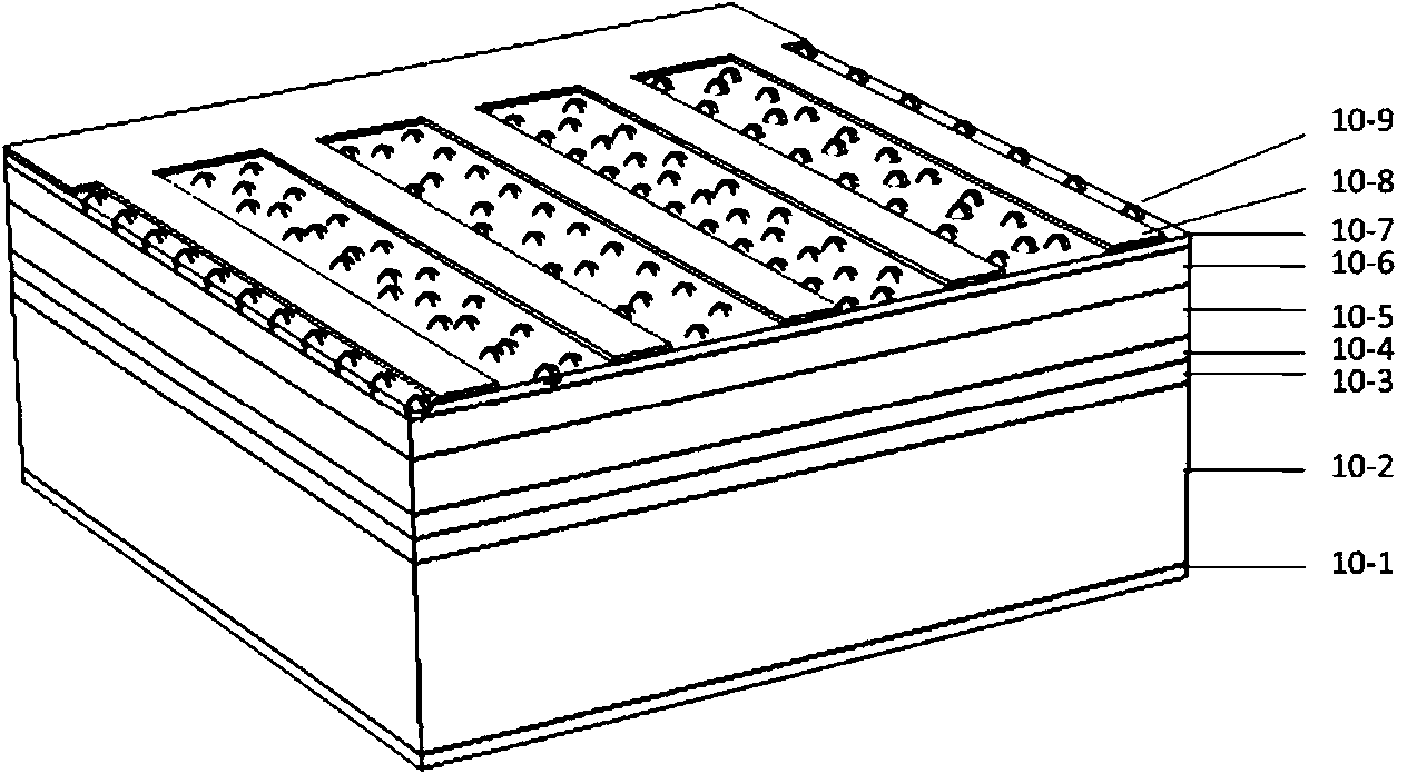
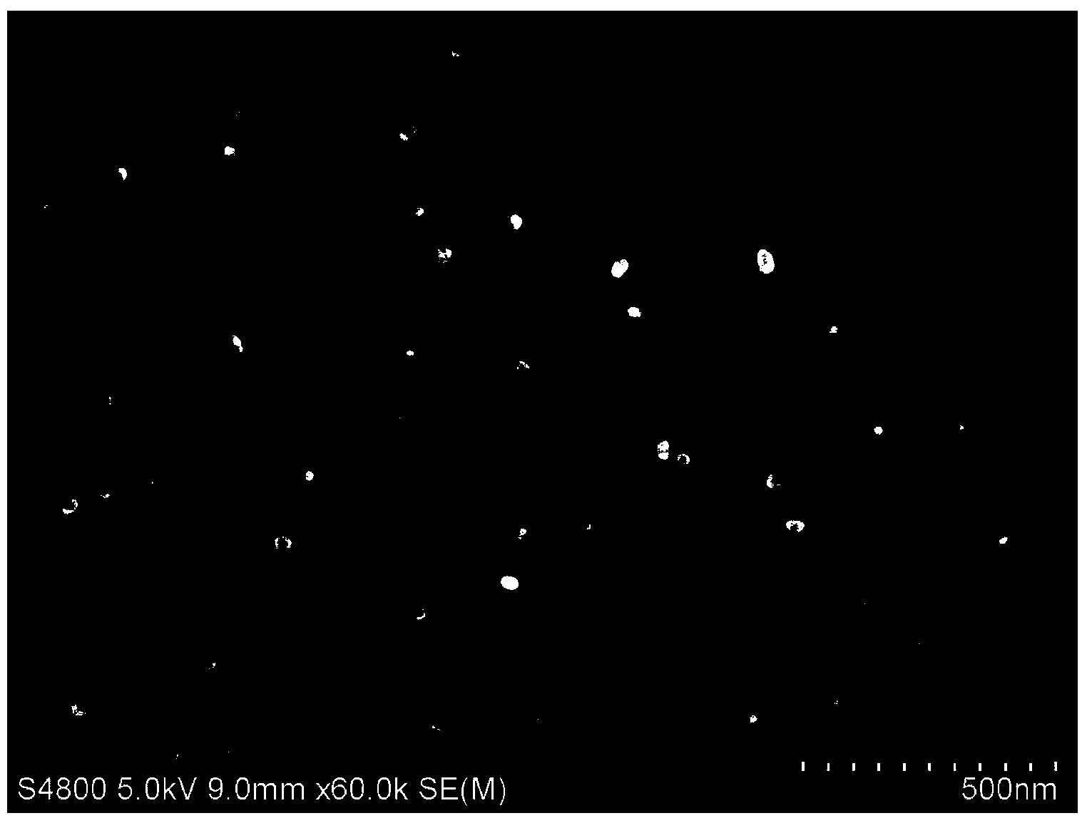
[0049] Such as Figure 1-Figure 3 shown.
[0050] A self-growing noble metal plasma unit nanostructure comprises the preparation of a noble metal nanostructure on the n-type AlInP layer on the surface of a solar cell.
[0051] The noble metal nanostructure is an Ag nanostructure, the diameter of the Ag nanostructure is 10-50 nm, and the distribution density of the Ag nanostructure is 2.0×10 9 -3.0×10 10 piece / cm 2 .
Embodiment 2
[0053] A self-growing noble metal plasmonic nanostructure as described in Example 1, the difference is that the noble metal nanostructure is an Au nanostructure, the diameter of the Au nanostructure is 20-70nm, and the Au nanostructure The distribution density of the structure is 1.0×10 10 -5.0×10 10 piece / cm 2 ; The Au nanostructure utilizes 1-5mM / LHAuCl 4 The solution reacts chemically with the n-type AlInP layer on the surface of the solar cell to prepare Au nanostructures.
Embodiment 3
[0055] As described in Example 1, a self-growth noble metal plasma element nanostructure is used, the difference is that the noble metal nanostructure is a Cu nanostructure, the diameter of the Cu nanostructure is 10-80nm, and the Cu nanostructure The distribution density of the structure is 1.0×10 9 -4.0×10 10 piece / cm 2 ; The Cu nanostructure utilizes CuCl of 5-50Mm / L 2 solution, Cu(NO 3 ) 2 solution or CuSO 4 The solution reacts chemically with the n-type AlInP layer on the surface of the solar cell to prepare Cu nanostructures.
PUM
| Property | Measurement | Unit |
|---|---|---|
| diameter | aaaaa | aaaaa |
| diameter | aaaaa | aaaaa |
| diameter | aaaaa | aaaaa |
Abstract
Description
Claims
Application Information


