
Obstruction film and manufacturing method thereof

A production method and barrier film technology, applied in semiconductor/solid-state device manufacturing, ion implantation plating, gaseous chemical plating, etc., can solve the problem that the service life of electronic components cannot meet the design requirements, increase production time and raw material consumption, barrier Low film barrier performance and other problems, to achieve the effect of low production cost, low water vapor transmission rate, and improve barrier performance

Inactive Publication Date: 2014-11-12
ZHANGJIAGANG KANGDE XIN OPTRONICS MATERIAL
View PDF8 Cites 33 Cited by
  • Summary
  • Abstract
  • Description
  • Claims
  • Application Information

AI Technical Summary

Problems solved by technology

[0005] Although technicians have done a lot of research on the barrier film, there are still many problems in the current barrier film technology: first, the barrier performance of the barrier film is still low, so that the service life of the electronic components cannot meet the design requirements. Continue to improve the barrier performance of the barrier film; second, the above barrier film is obtained by multi-layer compounding, adding particles or desiccant, which increases the production time and raw material consumption, and increases its production cost; third, the water vapor barrier film It is often damaged during transportation and use, so it is not suitable for use and installation

Method used

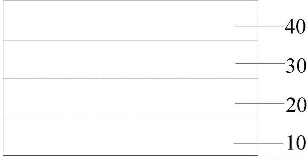
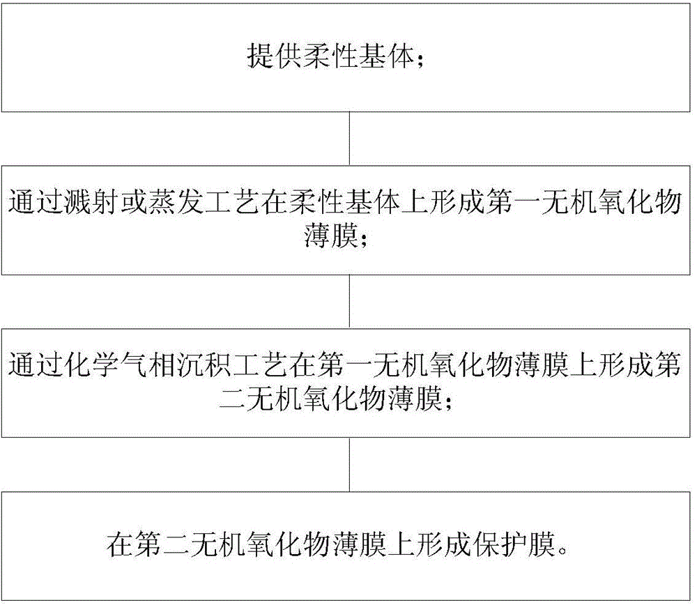
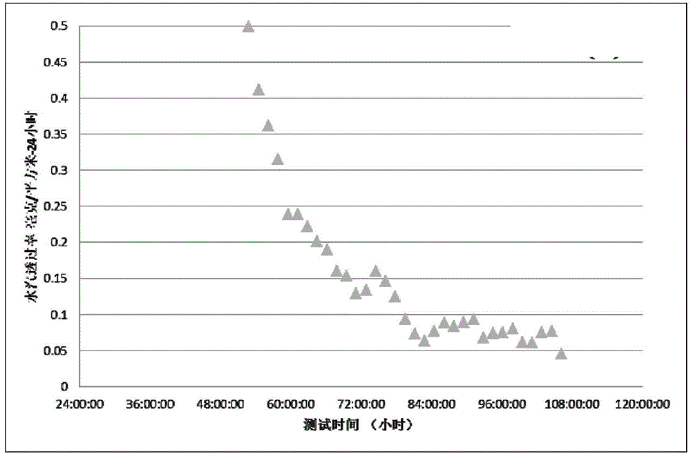

Image

  • Obstruction film and manufacturing method thereof
  • Obstruction film and manufacturing method thereof
  • Obstruction film and manufacturing method thereof

Examples


Embodiment 1

[0046] This embodiment provides a barrier film and a manufacturing method thereof. Wherein, the preparation method includes the following steps:

[0047] providing a flexible substrate composed of polyethylene terephthalate (PET), and coating the surface of the flexible substrate with a hardened coating composed of polyacrylate resin, wherein the thickness of the flexible substrate is 125 μm, and Through AFM detection, it can be seen that the surface roughness of the hardened coating is 1.24nm;

[0048] Forming a first inorganic oxide film on a flexible substrate by a sputtering process, wherein the material of the first inorganic oxide film is indium tin oxide (ITO), and the thickness of the first inorganic oxide film is 20nm;

[0049] A second inorganic oxide film is formed on the first inorganic oxide film by a chemical vapor deposition process, wherein the material of the second inorganic oxide film is Al 2 o 3 , the thickness of the second inorganic oxide film is 10 nm...


PUM

PropertyMeasurementUnit
Thicknessaaaaaaaaaa
Surface roughnessaaaaaaaaaa
Thicknessaaaaaaaaaa

Abstract

The invention discloses an obstruction film and a manufacturing method thereof. The obstruction film comprises a flexible base, a first inorganic oxide thin film, a second inorganic oxide thin film and a protective film, wherein the first inorganic oxide thin film is arranged on the flexible base, the second inorganic oxide thin film is arranged on the first inorganic oxide thin film, the protective film is arranged on the second inorganic oxide thin film, the first inorganic oxide thin film is formed by means of the sputtering or evaporating technology, and the second inorganic oxide thin film is formed by means of the chemical vapor deposition technology. The manufacturing method comprises the steps of providing the flexible base, forming the first inorganic oxide thin film on the flexible base through the sputtering or evaporating technology, forming the second inorganic oxide thin film on the first inorganic oxide thin film through the chemical vapor deposition technology, and forming the protective film on the second inorganic oxide thin film. The obstruction performance of the obstruction film can be improved, and the production cost of the obstruction film can be reduced.

Description

technical field [0001] The invention relates to the technical field of sealing of electronic components, in particular to a barrier film and a manufacturing method thereof. Background technique [0002] In the back-end process of electronic components, it is necessary to seal the electronic components so that the functional layers of the electronic components are separated from the water vapor, oxygen and other components in the atmosphere, and prevent the functional layers from reacting with water vapor and oxygen. Electronic components fail, thereby increasing the life of electronic components. For example, for organic light-emitting diodes (OLEDs), components such as water vapor and oxygen in the air can easily react with cathode metals (such as aluminum, magnesium, calcium, etc.) Components such as oxygen and oxygen will also chemically react with the hole transport layer and electron transport layer in the OLED, which will cause device failure. Therefore, effective en...

Claims


Application Information

Patent Timeline
IPC IPC(8): H01L51/52H01L51/56C23C28/04C23C14/08C23C16/40
CPCH01L23/291C23C28/00H10K50/844
Inventor 于甄胡坤
Owner ZHANGJIAGANG KANGDE XIN OPTRONICS MATERIAL
Learn More