
Semiconductor light-sensitive cell and semiconductor light-sensitive cell array thereof

A photosensitive unit, semiconductor technology, applied in the direction of semiconductor devices, transistors, electrical components, etc., can solve the problems affecting the working reliability and leakage of image sensor devices, and achieve the effect of small surface noise, preventing leakage of charges, and improving working reliability.

Active Publication Date: 2014-11-19
SUZHOU ORIENTAL SEMICONDUCTOR CO LTD
View PDF7 Cites 9 Cited by
  • Summary
  • Abstract
  • Description
  • Claims
  • Application Information

AI Technical Summary

Problems solved by technology

However, the semiconductor photosensitive devices of the above two structures that charge and discharge the floating gate through the photosensitive pn junction diode all have common problems: the photosensitive region of the photosensitive pn junction diode needs a large area, and the photosensitive region of the floating gate and the photosensitive pn junction diode It is directly connected, which makes the photosensitive current easily leak into the photosensitive area of ​​the photosensitive pn junction diode after being charged into the floating gate, which directly affects the working reliability of the image sensor device

Method used


Image

  • Semiconductor light-sensitive cell and semiconductor light-sensitive cell array thereof
  • Semiconductor light-sensitive cell and semiconductor light-sensitive cell array thereof
  • Semiconductor light-sensitive cell and semiconductor light-sensitive cell array thereof

Examples


Embodiment Construction

[0037] In order to clearly illustrate the specific implementation of the present invention, the diagrams listed in the drawings of the description enlarge the thickness of the layers and regions described in the present invention, and the listed figures do not represent the actual size; the drawings are schematic , should not limit the scope of the present invention. The embodiments listed in the description should not be limited to the specific shapes of the regions shown in the drawings, but include the obtained shapes such as deviations caused by manufacturing, etc., and the curves obtained by etching usually have curved or rounded characteristics, but All are represented by rectangles in the embodiments of the present invention. Also in the following description, the term substrate used may be understood to include the semiconductor wafer being processed, possibly including other thin film layers prepared thereon.

[0038] The specific implementation manners of the presen...


PUM


Abstract

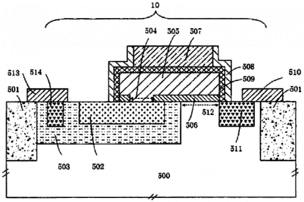
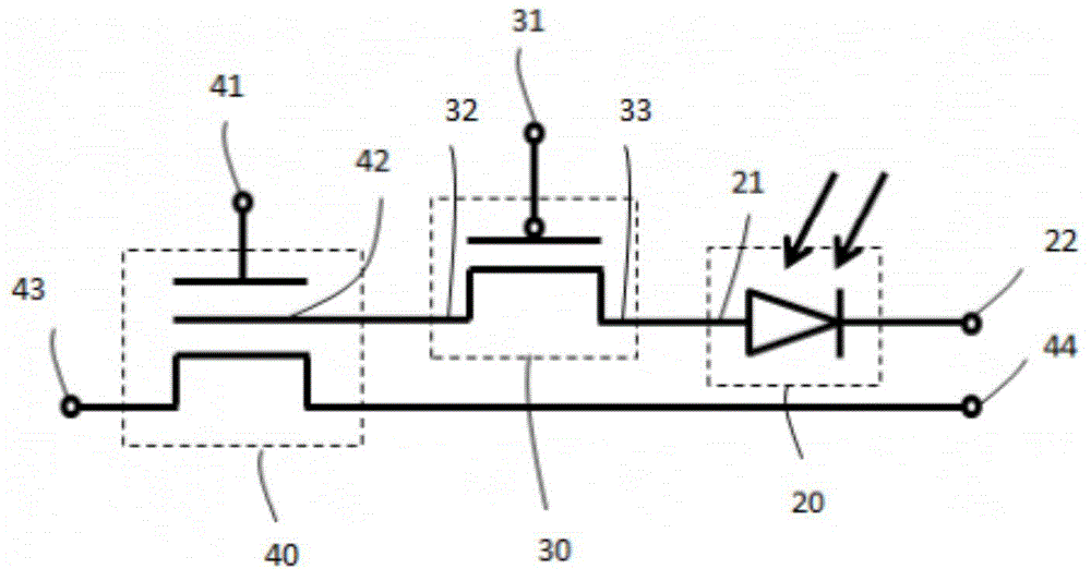
The invention relates to a semiconductor light-sensitive cell and a semiconductor light-sensitive cell array thereof. A floating gate transistor, a strobe MOS tube and a light-sensitive diode are disposed in a semiconductor substrate. An anode or cathode of the light-sensitive diode is connected to a floating gate of the floating gate transistor through the strobe MOS tube, and the corresponding cathode or anode of the light-sensitive diode is connected to a drain of the floating gate transistor or electrically connected to an external electrode. As for the semiconductor light-sensitive cell, after the strobe MOS tube is switched on, the floating gate is charged or discharged through the light-sensitive diode; and after the strobe MOS tube is switched off, the charge is stored in the floating gate of the floating gate transistor. The semiconductor light-sensitive cell has the advantages of small cell area, low surface noise, long floating gate storing charge time, large operating voltage dynamic range and the like.

Description

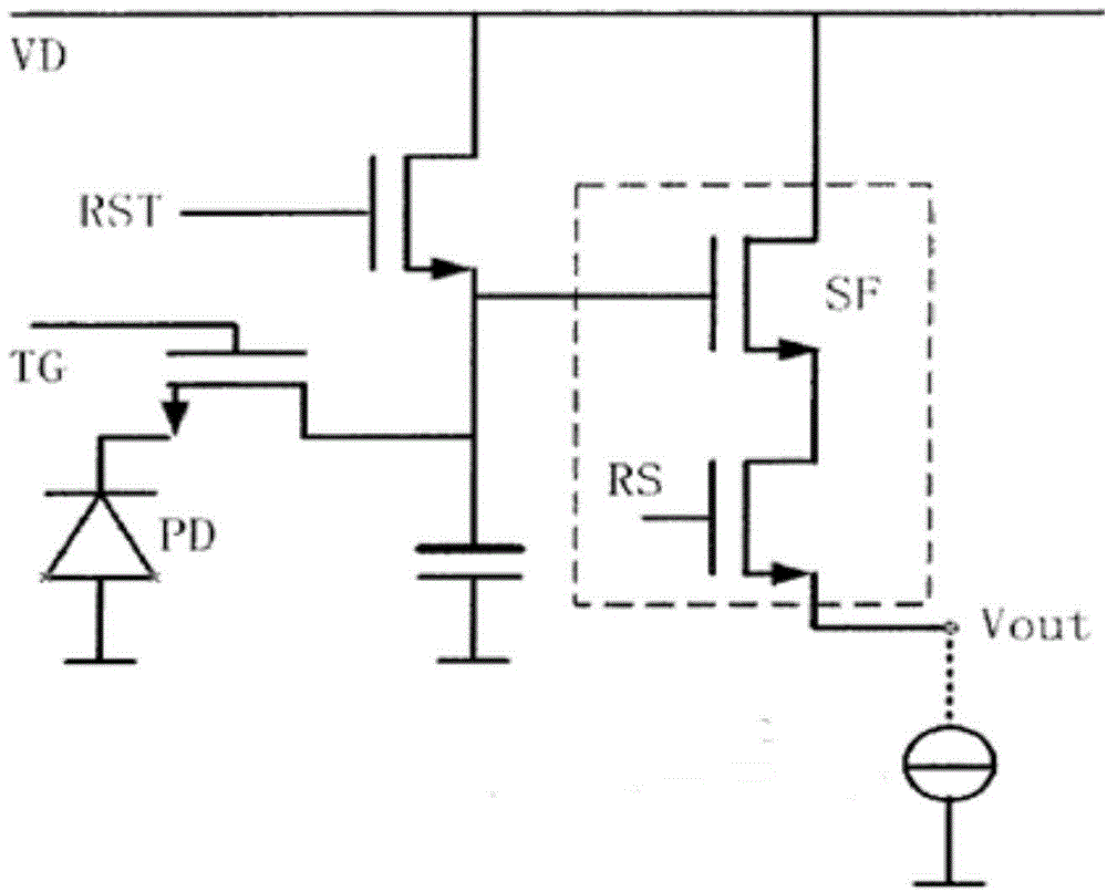
technical field [0001] The invention relates to a CMOS image sensor, in particular to a semiconductor photosensitive unit and a semiconductor photosensitive unit array thereof. Background technique [0002] There are currently two main types of image sensors: charge-coupled device image sensors and CMOS image sensors. The charge-coupled device image sensor has the advantages of high image quality and low noise, but its production cost is high, and it is not easy to integrate with peripheral circuits. The CMOS image sensor has high integration, small size, low power consumption, wide dynamic range, and is compatible with the manufacturing process of the charge-coupled device image sensor, which has the conditions of high system integration. Therefore, CMOS image sensors have become a research hotspot in recent years. [0003] figure 1 Shown is a CMOS image sensor composed of an existing single-pixel unit circuit. The single pixel unit of the CMOS image sensor is equipped w...

Claims


Application Information

Patent Timeline
Patent Type & Authority Applications(China)
IPC IPC(8): H01L27/146
CPCH01L27/14614H01L27/14603H01L27/14616H01L27/14636H01L27/14643H01L31/103H01L31/109
Inventor 刘伟刘磊王鹏飞
Owner SUZHOU ORIENTAL SEMICONDUCTOR CO LTD
Learn More