Internal-external double-electrode type miniature hemispherical resonance gyroscope and preparation method thereof
A technology of hemispherical resonant gyroscope and hemispherical resonant oscillator, which is applied in the direction of steering induction equipment, etc., can solve the problems of limited detection accuracy, undesigned leads and wire bonding pads, unfavorable signal application and signal extraction, etc., so as to improve detection accuracy and facilitate signal processing. Effect of application and signal extraction, increasing number of electrodes
- Summary
- Abstract
- Description
- Claims
- Application Information
AI Technical Summary
Problems solved by technology
Method used
Image
Examples
Embodiment 1
[0051] Such as Figure 2(a)-Figure 2(c) As shown, the present embodiment provides a kind of internal and external dual-electrode miniature hemispherical resonant gyroscope, comprising:
[0052] a single crystal silicon substrate 1;
[0053] a central fixed support column 2;
[0054] A miniature hemispherical harmonic oscillator 3;
[0055] Eight uniformly distributed external electrodes 4;
[0056] Eight external electrode metal welding plates 5;
[0057] a glass substrate 6;
[0058] Sixteen metal leads 7;
[0059] Sixteen round wire reels 8;
[0060] Eight external electrode metal connection columns 9;
[0061] Eight evenly distributed internal electrodes 10;
[0062] a seed layer 11;
[0063] Wherein: one end of the central fixed support column 2 is connected to the single crystal silicon substrate 1, and the other end is connected to the micro hemispherical resonator 3; the external electrode 4 is arranged on the lower surface of the single crystal silicon substra...
Embodiment 2
[0080] Such as Figure 1(a)-Figure 1(k) As shown, the present embodiment provides a method for preparing an internal and external dual-electrode miniature hemispherical resonant gyroscope, including the following steps:
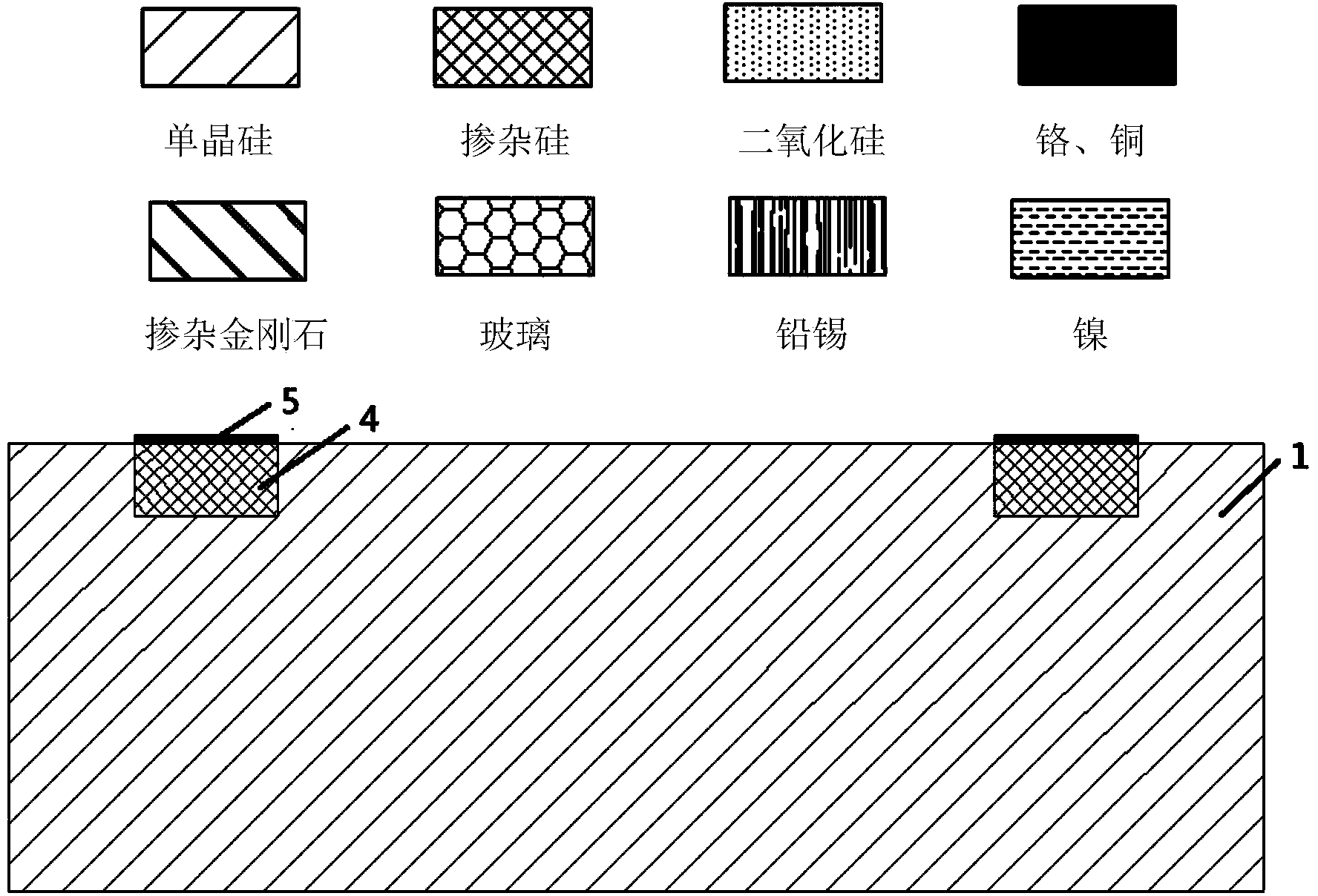
[0081] The first step, as shown in Figure 1(a), is to perform cleaning, glue coating, photolithography, development, boron ion implantation, sputtering, and glue removal processes on the single crystal silicon substrate to obtain a thickness on the single crystal silicon substrate 1. An external electrode 4 made of boron ion-doped silicon material with a thickness of 10 μm-50 μm and an external electrode metal welding plate 5 made of chromium and copper materials with a thickness of 50 nm-300 nm;
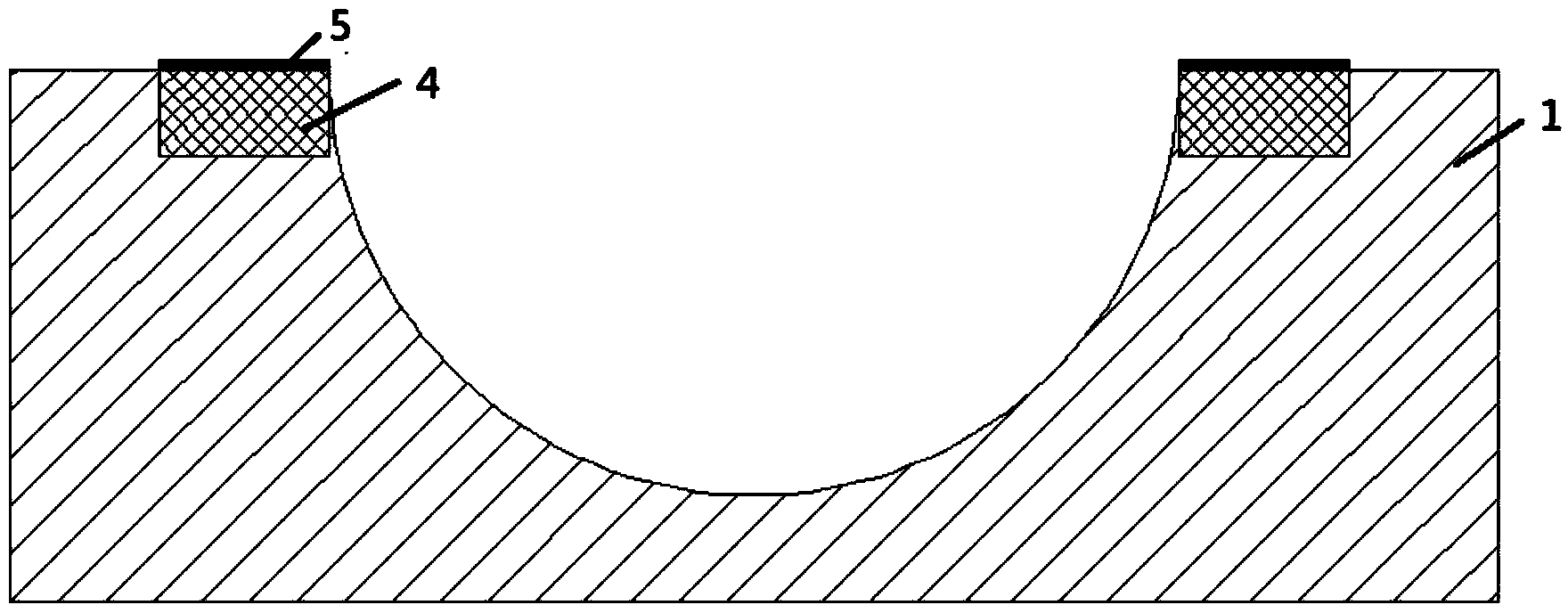
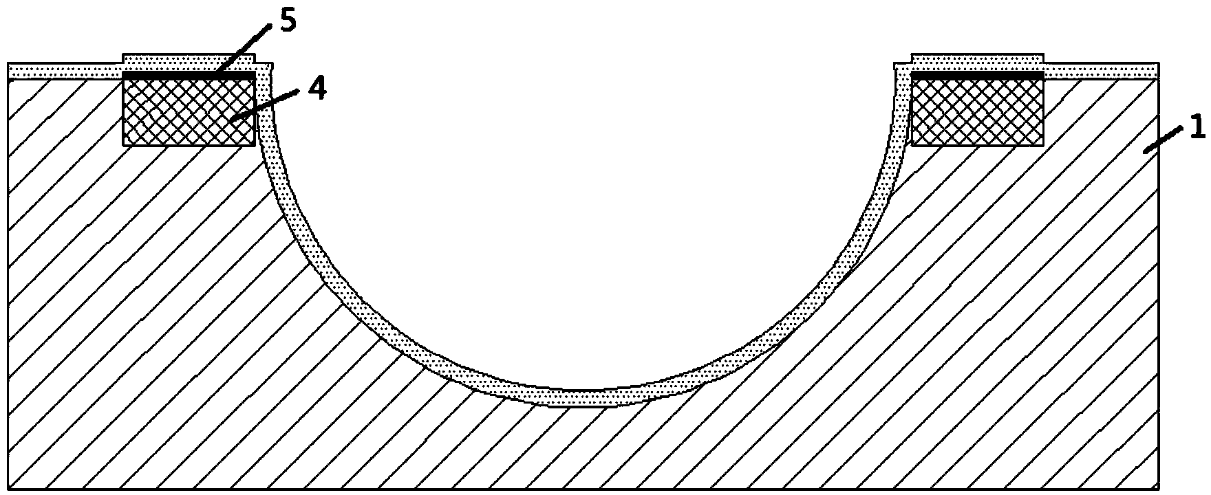
[0082] The second step, as shown in Figure 1(b), is based on the first step of glue coating, photolithography, development, silicon isotropic etching, and glue removal to obtain a radius on the single crystal silicon substrate 1. 300μm-700μm hemispherical groove; ...
Embodiment 3
[0094] Basically the same as embodiment 1 and embodiment 2, the difference is:
[0095] As shown in Fig. 3(a) and Fig. 3(b), the micro gyroscope prepared in this embodiment: the internal electrode 10 is a ring-shaped integrated electrode.
[0096] In this embodiment, the inner electrode 10 in the micro gyroscope can only provide a single control signal, and cannot apply a driving signal and extract a detection signal.
[0097] In this embodiment, the micro gyroscope can apply a ring control signal to the inner electrode 10, so that the micro gyroscope can work in the full-angle mode and directly detect the magnitude of the applied rotation angle.
PUM
| Property | Measurement | Unit |
|---|---|---|
| thickness | aaaaa | aaaaa |
| thickness | aaaaa | aaaaa |
| radius | aaaaa | aaaaa |
Abstract
Description
Claims
Application Information
 - R&D
- Intellectual Property
- Life Sciences
- Materials
- Tech Scout
- Unparalleled Data Quality
- Higher Quality Content
- 60% Fewer Hallucinations
Browse by: Latest US Patents, China's latest patents, Technical Efficacy Thesaurus, Application Domain, Technology Topic, Popular Technical Reports.
© 2025 PatSnap. All rights reserved.Legal|Privacy policy|Modern Slavery Act Transparency Statement|Sitemap|About US| Contact US: help@patsnap.com


