Thin film transistor, array substrate, and display device
A technology for thin film transistors and array substrates, applied in the display field, can solve the problems of large subthreshold swing of thin film transistors, affecting the conduction performance of thin film transistors, reducing carrier transfer rate, etc. The effect of communication performance and performance improvement
- Summary
- Abstract
- Description
- Claims
- Application Information
AI Technical Summary
Problems solved by technology
Method used
Image
Examples
Embodiment 1
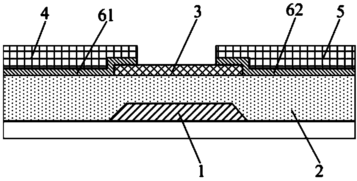
[0029] This embodiment provides a thin film transistor, such as figure 1 As shown, it includes gate 1, gate insulating layer 2, active layer 3, source 4 and drain 5, gate insulating layer 2 is arranged between gate 1 and active layer 3, source 4 and drain 5 Correspondingly arranged at both ends of the active layer 3, the active layer 3 is formed of a metal oxynitride material, and also includes a conductive oxygen vacancy reduction layer, and the oxygen vacancy reduction layer is arranged between the active layer 3 and the source electrode 4 , and the oxygen vacancy reduction layer is disposed between the active layer 3 and the drain electrode 5 for reducing the oxygen vacancies in the active layer 3 .
[0030] Among them, metal oxynitride materials such as zinc gallium oxynitride, zinc indium oxynitride, zinc aluminum oxynitride, zinc oxynitride (ZnON) and the like.
[0031] In this embodiment, the oxygen vacancy reduction layer includes a first reduction portion 61 and a se...
Embodiment 2
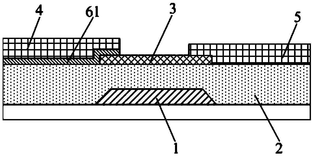
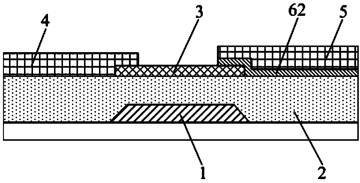
[0040] This embodiment provides a thin film transistor. The difference from Embodiment 1 is that the oxygen vacancy reduction layer in this embodiment only includes the first reduction portion 61 (such as figure 2 ), or, only the second cutting part 62 is provided in the present embodiment (as image 3 ).
[0041] Correspondingly, in figure 2When manufacturing the thin film transistor in , firstly, a pattern including the first cut portion 61 is formed through a patterning process, and then a pattern including the source 4 and the drain 5 is formed through a patterning process. exist image 3 When manufacturing the thin film transistor in , the pattern including the second cut portion 62 is firstly formed through a patterning process, and then the pattern including the source 4 and the drain 5 is formed through a patterning process.
[0042] Other structures and materials of the thin film transistor in this embodiment are the same as those in Embodiment 1, and will not be...
Embodiment 3
[0045] This embodiment provides a thin film transistor, which is different from Embodiment 1-2, such as Figure 4 As shown, the thin film transistor also includes an etch barrier layer 7, the etch barrier layer 7 is arranged between the active layer 3 and the source electrode 4 and the drain electrode 5, and the oxygen vacancy reduction layer is located at the edge of the etch barrier layer 7 away from the active layer 3; the etch stop layer 7 is provided with a first via hole 8 in the area corresponding to the first cut portion 61, and the first cut portion 61 is in contact with the active layer 3 through the first via hole 8; the etch stop A second via hole 9 is opened in the area of the layer 7 corresponding to the second cutout portion 62 , and the second cutout portion 62 is in contact with the active layer 3 through the second via hole 9 .
[0046] Other structures of the thin film transistor in this embodiment are the same as those in any one of Embodiments 1-2, and w...
PUM
 Abstract
Description
Claims
Application Information


