An electrochromic wo 3 Controlled Preparation of Thin Films
An electrochromic and thin film technology, applied in ion implantation plating, coating, metal material coating process, etc., can solve the problems of poor controllability, small optical modulation amplitude, and high integral transmittance of film coloring state, and achieve optical The effect of large modulation amplitude, low transmittance, and adjustable oxygen-deficient phase intensity
- Summary
- Abstract
- Description
- Claims
- Application Information
AI Technical Summary
Problems solved by technology
Method used
Image
Examples
Embodiment 1
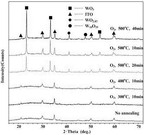
[0021] To clean the ITO conductive glass substrate, first clean the glass pieces in sequence with tap water and deionized water, then soak them in acetone and ethanol solutions successively, clean them with an ultrasonic cleaner for 15 minutes, and then put them in a drying box to dry; Preparation of WO by Beam Sputtering Deposition x Thin films, before sputtering deposition, use the method of "mechanical pump + molecular pump" to pump the basic vacuum of the chamber to 4.5×10 -3 Pa, and then pass high-purity argon gas with a purity of 99.999% and a flow rate of 16 sccm, and a working vacuum of 1.5×10 -2 Pa; in sputtering deposition, the accelerating voltage of sputtering ions is 2000V, the sputtering beam current is 60mA, and the deposition time is 3 hours, the prepared WO x The film thickness is about 280nm. Using 99.999% pure O 2 As an annealing atmosphere, at 500 o C temperature will WO x After the film was annealed for 10 minutes, the film crystallized into WO 3 Mai...
Embodiment 2
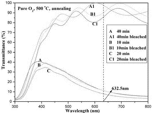
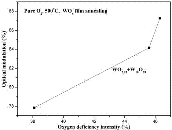
[0023]Under the same conditions in Example 1, at 500 o C temperature will WO x After annealing the film for 20 minutes, the film crystallized into WO 3 Main crystalline phase, accompanied by oxygen-deficient phase WO 2.83 and W 10 o 29 polycrystalline film ( figure 1 ); for WO 3 Li + Electrochemical coloring and fading reaction, the coloring time is about 20s; after applying ± 4V voltage coloring and fading treatment, WO 3 The optical modulation value of the film at 632.5nm wavelength is as high as 78% (see Table 1 and figure 2 ); the integral transmittance of the colored state for visible light is only 12%; the highest transmittance of the colored state is located at the wavelength of 414.5nm, and its value is only 34%; in the visible light range, the optical modulation values at each wavelength are greater than 50%, Optical modulation value varies with anoxic phase WO 2.83 and W 10 o 29 The total strength of the monotonically increasing trend ( image 3 ).
Embodiment 3
[0025] Under the same conditions in Example 1, at 500 o C temperature will WO x The film was annealed for 40 minutes, and the film crystallized into WO 3 Main crystalline phase, accompanied by oxygen-deficient phase WO 2.83 and W 10 o 29 polycrystalline film ( figure 1 ); for WO 3 Li + Electrochemical coloring and fading reaction, the coloring time is about 20s; after applying ± 4V voltage coloring and fading treatment, WO 3 The optical modulation value of the film at 632.5nm wavelength is as high as 87% (Table 1 and figure 2 ), in the visible light range, the optical modulation values at each wavelength are greater than 50%, and the optical modulation values increase with the oxygen-deficient phase WO 2.83 and W 10 o 29 The total strength of the monotonically increasing trend ( image 3 ).
[0026] Table 1
[0027]
PUM
| Property | Measurement | Unit |
|---|---|---|
| thickness | aaaaa | aaaaa |
Abstract
Description
Claims
Application Information


