Organic light emitting device and manufacturing method thereof

An electroluminescent device and electroluminescent technology, which are applied in the fields of electro-solid devices, semiconductor/solid-state device manufacturing, electrical components, etc., can solve the problems of low luminous efficiency and low electron transfer rate, and achieve high luminous efficiency and long service life. Effect

Inactive Publication Date: 2014-12-03
OCEANS KING LIGHTING SCI&TECH CO LTD +2
View PDF5 Cites 1 Cited by
  • Summary
  • Abstract
  • Description
  • Claims
  • Application Information

AI Technical Summary

Problems solved by technology

However, in current organic electroluminescent devices, the electron transport rate is low, resulting in low luminous efficiency of organic electroluminescent devices

Method used


Image

  • Organic light emitting device and manufacturing method thereof
  • Organic light emitting device and manufacturing method thereof
  • Organic light emitting device and manufacturing method thereof

Examples


preparation example Construction

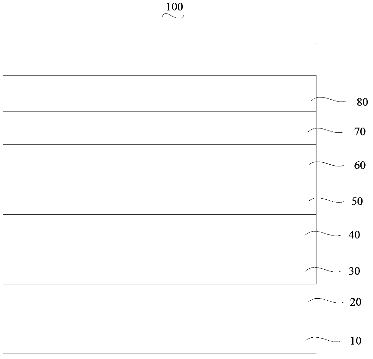
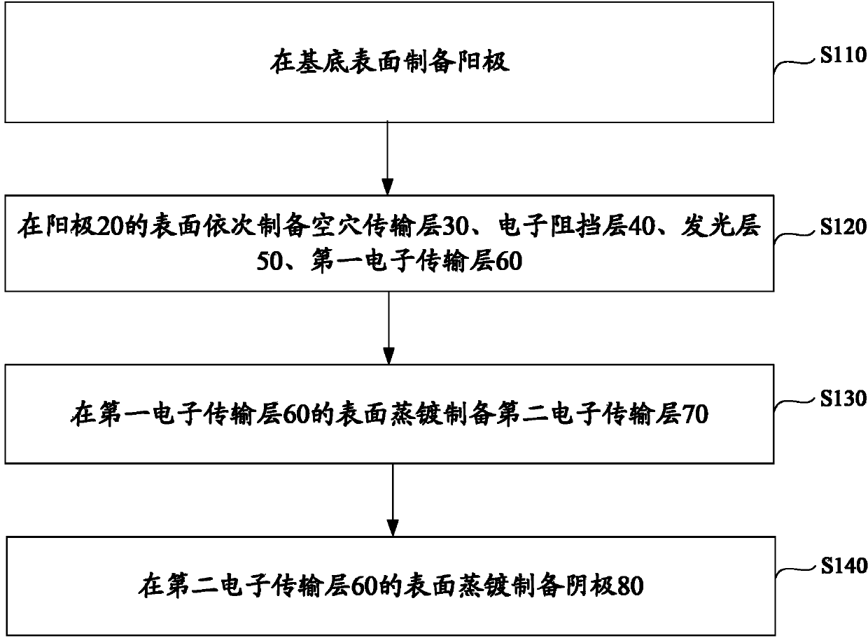
[0033] Such as figure 2 As shown, the manufacturing method of an organic electroluminescent device according to an embodiment includes the following steps:

[0034] In step S110, an anode 20 is prepared on the surface of the substrate 10.

[0035] The substrate 10 is glass.

[0036] The substrate 10 is pre-treated before use. The pre-treatment includes: placing the substrate in deionized water containing detergent for ultrasonic cleaning, and then using isopropanol, acetone in ultrasonic waves for 20 minutes after cleaning, and then using nitrogen. Blow dry.

[0037] The anode 20 is formed on the surface of the substrate 10. The material of the anode 20 is indium tin oxide (ITO) or aluminum doped zinc oxide (AZO). The thickness of the anode 20 is 70 nm to 200 nm.

[0038] In this embodiment, the anode 20 is prepared by vacuum sputtering. When sputtering, the background vacuum is 1×10 -5 Pa~1×10 -3 Pa, the sputtering rate is 0.2nm / s~1nm / s.

[0039] In step S120, the hole transport l...
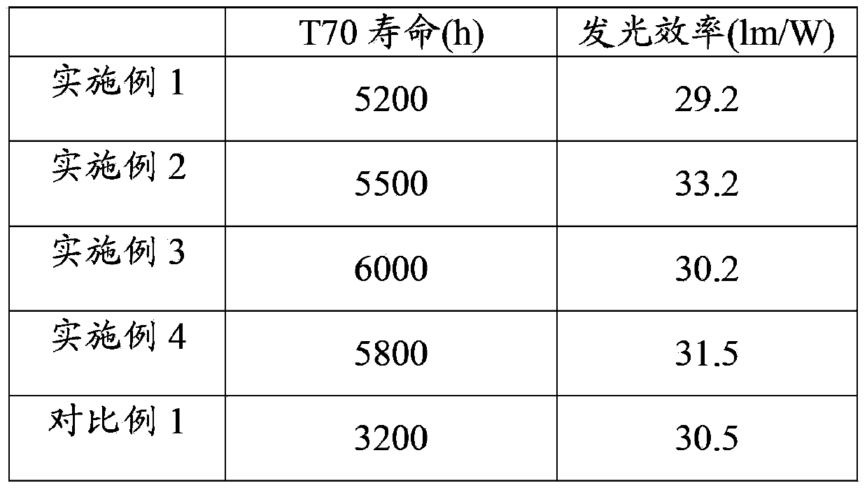
Embodiment 1

[0051] The structure of the organic electroluminescent device of this embodiment is: glass substrate / ITO(100nm) / F4-TCNQ: MeO-TPD(40nm) / TAPC(10nm) / Ir(ppy) 3 :CBP(10nm) / BEDT-TTF: NTCDA(30nm) / CsN 3 :TPBi(60nm) / Ag(100nm). Wherein, " / " means a laminated structure, and ":" means doping or mixing, and the following embodiments are the same.

[0052] In this preparation process, the working pressure of vacuum sputtering and vacuum evaporation is 1×10 -5 Pa, the vapor deposition rate of organic materials is 0.1nm / s, the vapor deposition rate of metals is 0.2nm / s, the vapor deposition rate of metal compounds is 0.1nm / s, and the sputtering rate of semiconductor oxide films is 0.2nm / s .

[0053] The preparation of the organic electroluminescent device of this embodiment is as follows:

[0054] Step 1. Provide a substrate, place the glass in deionized water containing detergent for ultrasonic cleaning, and then use isopropanol and acetone in ultrasonic for 20 minutes after cleaning, and then dry...

Embodiment 2

[0062] The structure of the organic electroluminescence device is: glass substrate / ITO(200nm) / F4-TCNQ: MeO-TPD(60nm) / TAPC(10nm) / Ir(ppy) 3 :CBP(20nm) / PyroninB: NTCDA(40nm) / Li 2 CO 3 :Alq 3 (10nm) / Ag(200nm).

[0063] In this preparation process, the working pressure of vacuum sputtering and vacuum evaporation is 1×10 -3 Pa, the vapor deposition rate of organic materials is 2 nm / s, the vapor deposition rate of metals is 2 nm / s, the vapor deposition rate of metal compounds is 0.5 nm / s, and the sputtering rate of semiconductor oxide films is 0.2 nm / s.

[0064] A manufacturing method of an organic electroluminescence device includes the following steps:

[0065] Step 1. Provide the substrate; place the glass in deionized water containing detergent for ultrasonic cleaning, and after cleaning, treat it with isopropanol and acetone in ultrasonic for 20 minutes, and then dry it with nitrogen;

[0066] Step 2: When the vacuum degree is 1×10 -3 In the Pa vacuum coating system, the magnetron sputte...


PUM


Abstract

The invention discloses an organic light emitting device, which comprises a substrate, an anode, a hole transmission layer, an electron blocking layer, a light emitting layer, a first electron transmission layer, a second electron transmission layer and a cathode stacked sequentially. Material of the first electron transmission layer comprises 1, 4, 5, 8-naphthalenetetracarboxylic dianhydride and a dopant doped in the 1, 4, 5, 8-naphthalenetetracarboxylic dianhydride, wherein the dopant selects at least one from ethylenedithiolo tetrathiafulvalene or pyronin B; and the material of the second electron transmission layer comprises electron transmission material and alkali metal compounds doped in the electron transmission material. The light emitting efficiency of the organic light emitting device is high. The invention also provides an organic light emitting device manufacturing method.

Description

Technical field [0001] The invention relates to the field of electronic devices, in particular to an organic electroluminescent device and a preparation method thereof. Background technique [0002] The light-emitting principle of organic electroluminescent devices is based on the fact that electrons are injected from the cathode to the lowest unoccupied molecular orbital (LUMO) of organic matter under the action of an external electric field, and holes are injected from the anode to the highest occupied orbital (HOMO) of organic matter. Electrons and holes meet and recombine in the light-emitting layer to form excitons. The excitons migrate under the action of an electric field, transfer energy to the luminescent material, and excite the electrons to transition from the ground state to the excited state. The excited state energy is deactivated by radiation to produce photons , Release light energy. However, in current organic electroluminescent devices, the transmission rate of...

Claims


Application Information

Patent Timeline
Patent Type & Authority Applications(China)
IPC IPC(8): H01L51/54H01L51/56
CPCH10K85/621H10K50/165H10K50/11H10K71/00
Inventor 周明杰冯小明张娟娟王平
Owner OCEANS KING LIGHTING SCI&TECH CO LTD
Why Eureka
Try Eureka