Method for regulating and controlling LED epitaxial wafer wavelength uniformity through buffer layer
An LED epitaxial wafer and adjustment control technology, which is applied in semiconductor/solid-state device manufacturing, electrical components, circuits, etc., can solve the problems of low Bin drop rate, quality fluctuation, and chip wavelength distribution dispersion, and achieve accurate quantification of warpage adjustment. , reduce uncertainties, and improve the effect of product uniformity
- Summary
- Abstract
- Description
- Claims
- Application Information
AI Technical Summary
Problems solved by technology
Method used
Image
Examples
Embodiment 1
[0028] The inventive principle of the present invention is: the warpage of sapphire pattern substrate is mainly influenced by specification factors such as the depth of its pattern, spacing, and the control of buffer layer thickness can directly influence GaN layer to form crystal nucleus (or crystal nucleus) on pattern substrate surface. species) density and size, and then change the stress distribution of the buffer layer to the three-dimensional growth stage. Since the warpage during the growth of multiple quantum wells is closely related to the stress distribution of the buffer layer to the three-dimensional growth stage, it can be achieved by buffering The adjustment of the layer thickness effectively acts on the growth condition control of the multi-quantum well stage.
[0029] The method of the present invention adopts Metal Organic Chemical Vapor Deposition (MOCVD, Metalorganic Chemical Vapor Deposition) growth, and Veeco MOCVD cooperates with a sapphire patterned subst...
Embodiment 2
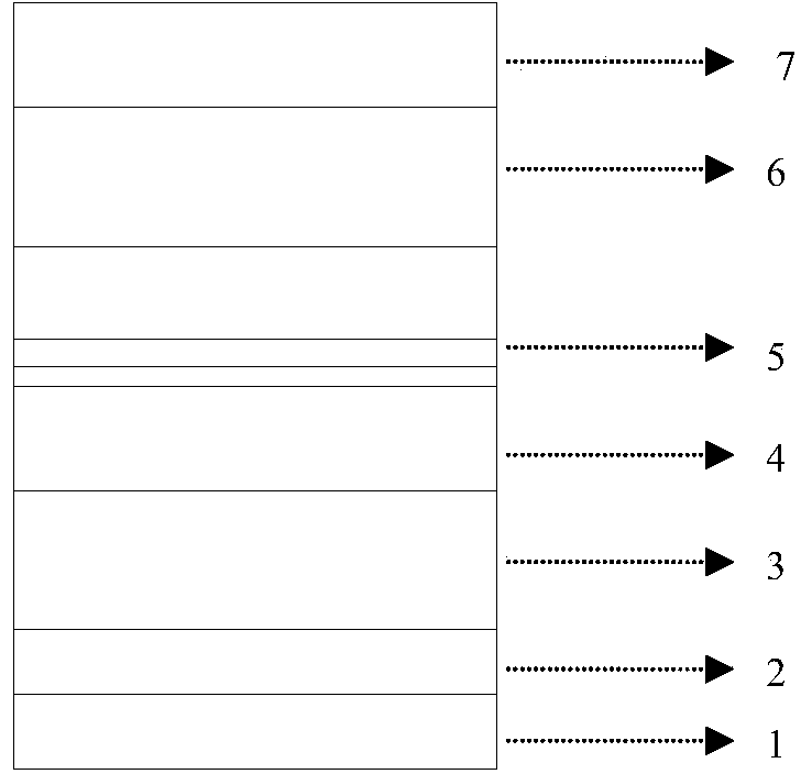
[0054] In this embodiment, the wavelength uniformity structure of the LED epitaxial wafer controlled by buffer layer adjustment is as follows from bottom to top: substrate, GaN buffer layer, non-doped GaN layer, N-type GaN layer, multiple quantum well layer, P-type AlGaN layer, For the P-type GaN layer, the thickness of the GaN buffer layer is such that the number and size of crystal nuclei formed on the surface of the substrate can be precisely controlled by adjusting the growth time, and the growth time of the buffer layer is 2 minutes.
[0055] Preferably, the multiple quantum well layer is In x Ga (1-x) N / GaN multiple quantum well layer, x=0.20-0.21, In x Ga (1-x) The thickness of the N layer is 3nm, the thickness of the GaN layer is 10nm, and the In x Ga (1-x) The period number of the N / GaN multi-quantum well layer is 13.
[0056] Steps c, d, e, f, g, and h of the method for controlling the wavelength uniformity of LED epitaxial wafers through buffer layer adjustment...
Embodiment 3
[0061] In this embodiment, the wavelength uniformity structure of the LED epitaxial wafer controlled by buffer layer adjustment is as follows from bottom to top: substrate, GaN buffer layer, non-doped GaN layer, N-type GaN layer, multiple quantum well layer, P-type AlGaN layer, For the P-type GaN layer, the thickness of the GaN buffer layer is such that the number and size of crystal nuclei formed on the surface of the substrate can be precisely controlled by adjusting the growth time, and the growth time of the buffer layer is 2 minutes.
[0062] Steps c, d, e, f, g, and h of the method for controlling the wavelength uniformity of LED epitaxial wafers through buffer layer adjustment in this embodiment are the same as in embodiment 1, and steps a and b include:
[0063] a. High temperature treatment of the sapphire patterned substrate in a hydrogen atmosphere at 1000-1100°C for 8-10 minutes;
[0064] b. Cool down to 545°C, feed 119sccm of TMGa and 56sccm of NH 3 , growing the...
PUM
| Property | Measurement | Unit |
|---|---|---|
| Thickness | aaaaa | aaaaa |
| Thickness | aaaaa | aaaaa |
| Thickness | aaaaa | aaaaa |
Abstract
Description
Claims
Application Information


