A method of controlling the wavelength uniformity of LED epitaxial wafers by adjusting the buffer layer

An LED epitaxial wafer and adjustment control technology, which is applied in semiconductor/solid-state device manufacturing, electrical components, circuits, etc., can solve the problems of low Bin drop rate, quality fluctuation, and uneven wavelength distribution, and achieve precise quantification of warpage adjustment. , Improve product uniformity, reduce the effect of uncertain factors

Active Publication Date: 2017-01-18
XIANGNENG HUALEI OPTOELECTRONICS
View PDF5 Cites 0 Cited by
  • Summary
  • Abstract
  • Description
  • Claims
  • Application Information

AI Technical Summary

Problems solved by technology

[0003] At present, domestic MOCVD using sapphire patterned substrates to grow LED epitaxial wafers will encounter fluctuations in quality due to switching between different types of sapphire patterned substrates, and differences in substrate pattern depth, spacing and other specifications lead to product growth process. The warping changes in the middle affect the uniformity of the wavelength distribution. The products grown under the original conditions are prone to the phenomenon that the wavelengths are longer or shorter than the concentric circles, resulting in non-concentrated wavelength distribution. Low
The existing technology solution is mainly to adjust the stress for the modification of the growth parameters between the epitaxial layers. The obvious disadvantage is that the wavelength uniformity of the product is not easy to control, and it is easy to cause changes in other photoelectric parameters other than the wavelength, which affects the quality parameters.

Method used


Image

  • A method of controlling the wavelength uniformity of LED epitaxial wafers by adjusting the buffer layer
  • A method of controlling the wavelength uniformity of LED epitaxial wafers by adjusting the buffer layer
  • A method of controlling the wavelength uniformity of LED epitaxial wafers by adjusting the buffer layer

Examples


Embodiment 1

[0028] The inventive principle of the present invention is: the warpage of sapphire pattern substrate is mainly influenced by specification factors such as the depth of its pattern, spacing, and the control of buffer layer thickness can directly influence GaN layer to form crystal nucleus (or crystal nucleus) on pattern substrate surface. species) density and size, and then change the stress distribution of the buffer layer to the three-dimensional growth stage. Since the warpage during the growth of multiple quantum wells is closely related to the stress distribution of the buffer layer to the three-dimensional growth stage, it can be achieved by buffering The adjustment of the layer thickness effectively acts on the growth condition control of the multi-quantum well stage.

[0029] The method of the present invention adopts Metal Organic Chemical Vapor Deposition (MOCVD, Metalorganic Chemical Vapor Deposition) growth, and Veeco MOCVD cooperates with a sapphire patterned subst...

Embodiment 2

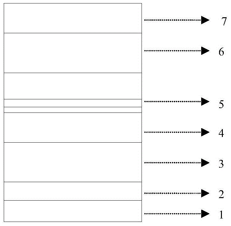
[0054] In this embodiment, the wavelength uniformity structure of the LED epitaxial wafer controlled by buffer layer adjustment is as follows from bottom to top: substrate, GaN buffer layer, non-doped GaN layer, N-type GaN layer, multiple quantum well layer, P-type AlGaN layer, For the P-type GaN layer, the thickness of the GaN buffer layer is such that the number and size of crystal nuclei formed on the surface of the substrate can be precisely controlled by adjusting the growth time, and the growth time of the buffer layer is 2 minutes.

[0055] Preferably, the multiple quantum well layer is In x Ga (1-x) N / GaN multiple quantum well layer, x=0.20-0.21, In x Ga (1-x) The thickness of the N layer is 3nm, the thickness of the GaN layer is 10nm, and the In x Ga (1-x) The period number of the N / GaN multi-quantum well layer is 13.

[0056] Steps c, d, e, f, g, and h of the method for controlling the wavelength uniformity of LED epitaxial wafers through buffer layer adjustment...

Embodiment 3

[0061] In this embodiment, the wavelength uniformity structure of the LED epitaxial wafer controlled by buffer layer adjustment is as follows from bottom to top: substrate, GaN buffer layer, non-doped GaN layer, N-type GaN layer, multiple quantum well layer, P-type AlGaN layer, For the P-type GaN layer, the thickness of the GaN buffer layer is such that the number and size of crystal nuclei formed on the surface of the substrate can be precisely controlled by adjusting the growth time, and the growth time of the buffer layer is 2 minutes.

[0062] Steps c, d, e, f, g, and h of the method for controlling the wavelength uniformity of LED epitaxial wafers through buffer layer adjustment in this embodiment are the same as in embodiment 1, and steps a and b include:

[0063] a. High temperature treatment of the sapphire patterned substrate in a hydrogen atmosphere at 1000-1100°C for 8-10 minutes;

[0064] b. Cool down to 545°C, feed 119sccm of TMGa and 56sccm of NH 3 , growing the...


PUM


Abstract

The invention discloses a method for regulating and controlling LED epitaxial wafer wavelength uniformity through a buffer layer. The steps of growing of a substrate, the GaN buffer layer, a non-doping GaN layer, an N-type GaN layer, a multiple quantum well layer, a P-type AlGaN layer and a P-type GaN layer are sequentially involved in the method. The method is characterized by including that deposit rate of the GaN buffer layer on the surface of the substrate is controlled by regulating the growing time, and growing of the GaN layer is performed by cooperating with decomposition and the decomposition of the GaN layer in the recrystallization stage, wherein variation in thickness in growing of the GaN layer corresponds to wavelength difference of a central zone and an edge of a epitaxial wafer. The purpose of controlling the wavelength uniformity can be realized by controlling the growing time of the LED epitaxial wafer buffer layer.

Description

technical field [0001] The invention belongs to the technical field of semiconductors and relates to a method for adjusting and controlling the wavelength uniformity of an LED epitaxial wafer through a buffer layer. Background technique [0002] Gallium nitride-based materials, including InGaN, GaN, and AlGaN alloys, are direct bandgap semiconductors, and the bandgap is continuously adjustable from 1.8-6.2eV. They have excellent properties such as wide direct bandgap, strong chemical bonds, high temperature resistance, and corrosion resistance. It is an ideal material for the production of short-wavelength high-brightness light-emitting devices, ultraviolet light detectors and high-temperature and high-frequency microelectronic devices. It is widely used in full-color large-screen displays, LCD backlights, signal lights, lighting and other fields. [0003] At present, domestic MOCVD using sapphire patterned substrates to grow LED epitaxial wafers will encounter fluctuations ...

Claims


Application Information

Patent Timeline
Patent Type & Authority Patents(China)
IPC IPC(8): H01L33/00H01L33/12
CPCH01L21/0242H01L21/02458H01L21/0254H01L21/0262H01L33/0066H01L33/0075H01L33/12
Inventor 涂靓虎吴际
Owner XIANGNENG HUALEI OPTOELECTRONICS
Why Eureka
Try Eureka