Platinum diselenide crystal material and preparation method thereof

A technology of selenization and platinum crystals, applied in the field of nanomaterials, can solve the problems of lack of energy gap in electronic structure and no reports

Active Publication Date: 2014-12-24
INST OF PHYSICS - CHINESE ACAD OF SCI
View PDF1 Cites 23 Cited by
  • Summary
  • Abstract
  • Description
  • Claims
  • Application Information

AI Technical Summary

Problems solved by technology

However, graphene has its inherent flaw: the lack of energy gaps in the electronic structure
[0005] As a member of the family of transition metal dichalcogenides, it has been theoretically predicted that the electronic energy band of platinum diselenide materials has achieved a half-metal-semiconductor transition from bulk to monolayer, making it widely used in photocatalysis and other fields. However, there is no report about its experimental preparation method, especially the preparation of samples with a single layer thickness.

Method used


Image

  • Platinum diselenide crystal material and preparation method thereof
  • Platinum diselenide crystal material and preparation method thereof
  • Platinum diselenide crystal material and preparation method thereof

Examples


Embodiment Construction

[0024] The specific implementation of the platinum diselenide crystal material provided by the present invention and its preparation method will be described in detail below in conjunction with the accompanying drawings.

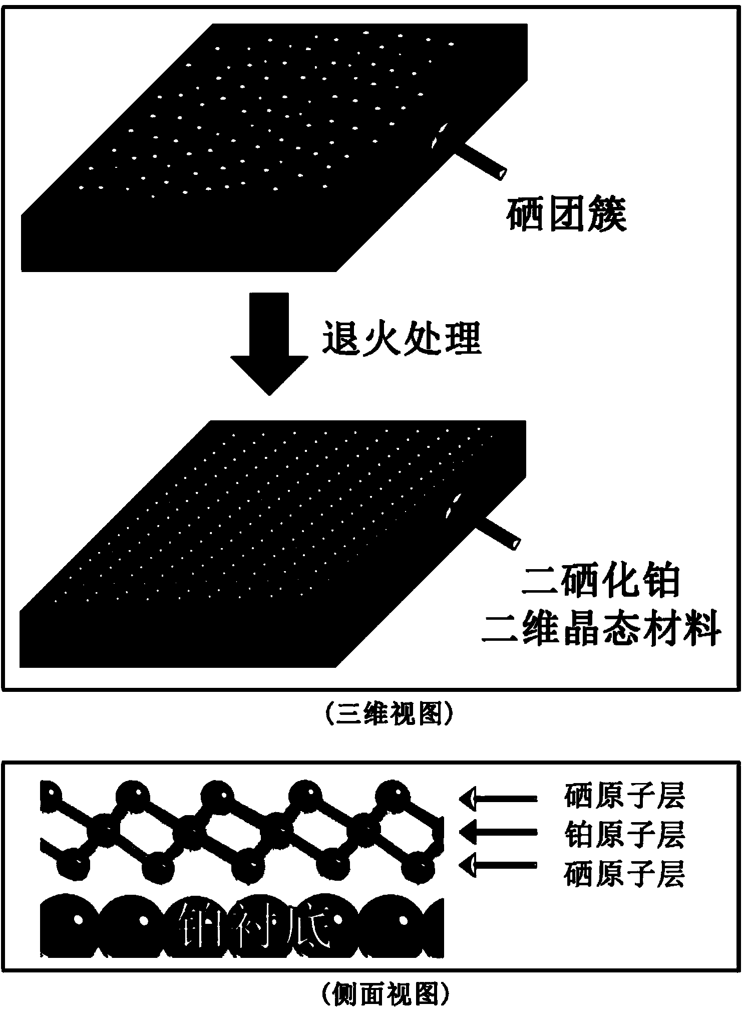
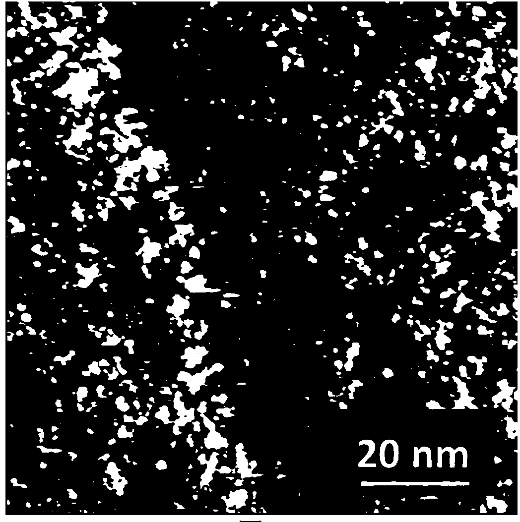
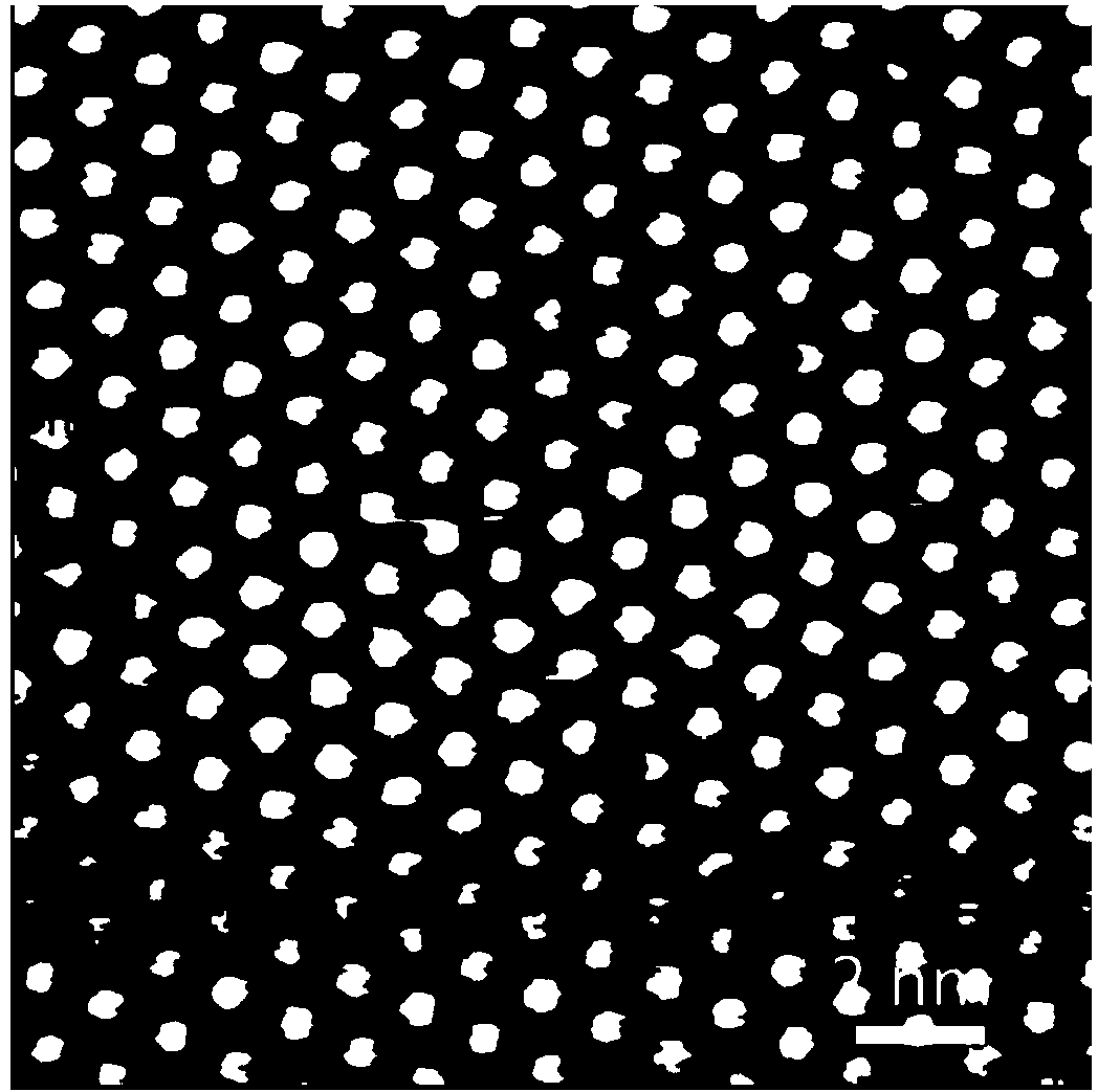
[0025] This example is to prepare a high-quality two-dimensional platinum diselenide crystalline material on the surface of a transition metal. The schematic diagram of the overall preparation process is as follows: figure 1 shown. In the three-dimensional view, the upper part of the figure shows the high-coverage selenium particles deposited at room temperature on the (111) surface of platinum in the present invention; the lower part of the figure shows the surface of the platinum (111) A two-dimensional ordered platinum diselenide crystalline material grown on the surface. In the side view, the arrangement of platinum diselenide on the substrate surface is clearly represented, where the atomic layers of selenium and platinum are formed as a sandwich stru...


PUM


Abstract

The invention discloses a platinum diselenide crystal material and a preparation method thereof. The preparation method comprises the following steps: 1) under a vacuum environment, evaporating and depositing a proper amount of high purity selenium on a metal platinum substrate; and 2) carrying out an annealing treatment, so that selenium atoms covering the surface of the substrate and platinum atoms on the substrate interact to form a two-dimensional ordered crystalline state membrane structure in a sandwich arrangement of selenium-platinum-selenium so as to obtain the platinum diselenide crystal material. The inorganic two-dimensional crystalline state material is a new member of a transitional metal disulfide compound family, expands the field of research on non-carbon based two-dimensional crystal materials, and has a wide application potential in future information electronics and apparatus development and research. According to the method disclosed by the invention, the platinum diselenide two-dimensional crystalline state material with a big area and a high quality is grown on a molecular beam epitaxial method, so that the electronic properties of the platinum diselenide crystalline state material and related applications and development are favorably researched.

Description

technical field [0001] The invention relates to a transition metal dichalcogen compound two-dimensional crystal material and a preparation method thereof, belonging to the technical field of nanometer materials. Background technique [0002] Graphene, as a classic representative of two-dimensional atomic crystal materials, has been successfully stripped from its parent graphite in 2004. Due to its unique electronic and physical properties, it has become a research hotspot that has attracted worldwide attention in the past ten years, triggering worldwide attention. There is an upsurge in the exploration and research of new two-dimensional crystal materials. The strange physical properties of graphene come from its unique electronic structure: the linear dispersion relationship near the K point in the momentum space makes its carriers can be regarded as massless Dirac fermions, which brings a series of new physical properties . Graphene's excellent physical properties such a...

Claims


Application Information

Patent Timeline
Patent Type & Authority Applications(China)
IPC IPC(8): C23C14/58C23C14/06
Inventor 王业亮李林飞王裕祺高鸿钧
Owner INST OF PHYSICS - CHINESE ACAD OF SCI
Why Eureka
Try Eureka