Plated copper wire structure used for ultrasonic bonding

A technology of ultrasonic wave and bonding wire, applied in the direction of electrical components, electric solid devices, circuits, etc., can solve problems such as poor bonding and difficult to improve the reliability evaluation of the second bonding

Inactive Publication Date: 2014-12-24
TANAKA DENSHI KOGYO KK
View PDF23 Cites 13 Cited by
  • Summary
  • Abstract
  • Description
  • Claims
  • Application Information

AI Technical Summary

Problems solved by technology

In addition, even if the film thickness is based on the nanometer level, "if the outer layer thickness is less than 20nm, the effect of inhibiting oxidation will be small, so bonding failure will also occur during wedge bonding, and it will be difficult to improve the quality of the second bonding." Reliability Evaluation" (claim 1 and paragraph 0053 of JP-A-2009-140953 Gazette), etc., so far, the plated copper wires are completely isolated from the core material and the atmosphere by coating.

Method used


Image

  • Plated copper wire structure used for ultrasonic bonding
  • Plated copper wire structure used for ultrasonic bonding
  • Plated copper wire structure used for ultrasonic bonding

Examples


Embodiment

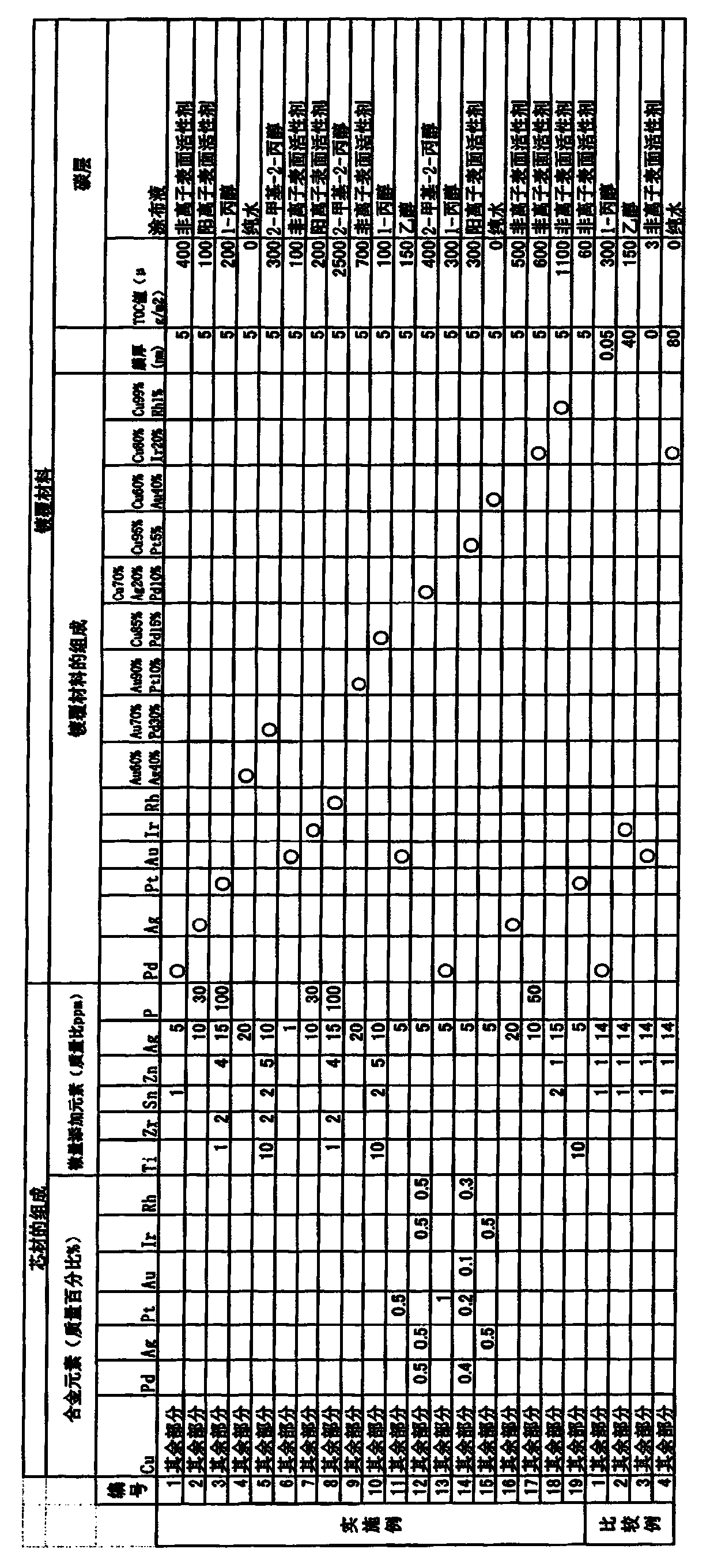
[0068] With the pure copper alloy wire (copper (Cu) and silver (Ag) are more than 99.9999% by mass percentage purity of composition of core material and plating material shown in Table 1, other alloy components are respectively more than 99.99% by mass percentage purity) After uniform melting and casting, rolling was performed while performing intermediate heat treatment to obtain a thick wire with a diameter of 1 mm. Grooves of sub-µm to several µm are formed on the outer periphery of the thick wire, and a plating material is plated thereon. Then, the wire is continuously drawn through a diamond die by wet method, and finally a 15 μm bonding wire is obtained. The theoretical film thicknesses of the products of Examples 1 to 19 are all 5 nm. In addition, the average diameter reduction rate is 6 to 20%, and the final linear velocity is 100 m / min.

[0069] In addition, the bonding wire used for the second window test and surface morphology imaging of the example products descr...


PUM

PropertyMeasurementUnit
diameteraaaaaaaaaa
mean roughnessaaaaaaaaaa
diameteraaaaaaaaaa

Abstract

The invention provides a plated copper wire structure used for ultrasonic bonding, through which even if plating materials of plated copper wires or core material types and wire diameters are changed , ultrasonic bonding can be stably carried out with a broad process window when a bonding condition is not individually set. The structural characteristics of the plated copper wire structure used for the ultrasonic bonding are that the surface morphology is that a plurality of cirrus-cloud-shaped grooves along length direction of a bonding wire are molded in the surface of the core materials; the core materials are plated with plating materials composed of precious metal or alloy (which is briefly referred to as precious metal, etc. ) which are with better inoxidizability than the inoxidizability of the core materials.

Description

technical field [0001] The present invention relates to a coated copper alloy wire for ultrasonic bonding (ultrasonic bonding) suitable for connecting IC chip electrodes used in semiconductor devices to circuit boards such as external leads, especially in high-temperature environments such as automotive applications, power semiconductors, and high-speed equipment applications. Bonding impacting wires for ultrasonic bonding used below, or copper-plated bonding wires for air-free balls (FAB) that are used even for ultra-fine wires of 15 μm or less. Background technique [0002] Various types of copper wires for connecting IC chip electrodes and external leads of semiconductor devices have been developed. For example, there are pure copper alloy wires that add titanium (Ti) or zirconium (Zr) (JP-A 62-102551), add boron (B) (JP-A-62-102552), and add magnesium (Mg) (JP-A). 62-130248), added rare earth elements (including yttrium (Y)) (JP 62-193254), added calcium (Ca) (JP 62-102...

Claims


Application Information

Patent Timeline
Patent Type & Authority Applications(China)
IPC IPC(8): H01L23/49C25D7/06
CPCH01L24/43H01L2224/43H01L2224/43848H01L2224/45H01L2224/45014H01L2224/45015H01L2224/45147H01L2224/45565H01L2224/85207H01L2924/181H01L2924/01203H01L2924/00H01L2924/00014H01L2924/00012H01L2924/01046H01L2924/01047H01L2924/01078H01L2924/01079H01L2924/01077H01L2924/01045H01L2924/01022H01L2924/0104H01L2924/0105H01L2924/0103H01L2924/206
Inventor 三上道孝刘斌天野裕之滨本拓也今泉欣之永江祐佳山下勉
Owner TANAKA DENSHI KOGYO KK
Why Eureka
Try Eureka