A kind of non-volatile three-dimensional semiconductor memory and its preparation method

A non-volatile, semi-conductive technology, applied in the direction of semiconductor devices, electrical solid-state devices, electrical components, etc., can solve the problems of short-channel effect, different doping concentration, etc., achieve enhanced control ability, good thermal stability, and avoid short-circuit ditch effect

Active Publication Date: 2017-04-26
HUAZHONG UNIV OF SCI & TECH
View PDF4 Cites 0 Cited by
  • Summary
  • Abstract
  • Description
  • Claims
  • Application Information

AI Technical Summary

Problems solved by technology

[0007] Aiming at the defects of the prior art, the object of the present invention is to provide a non-volatile three-dimensional semiconductor memory and its preparation method, aiming to solve the problem of the source, drain and channel regions having different doping concentrations in the prior art, which makes the source, drain, and channel regions There is a PN junction between the drain region and the channel region, which leads to the problem of short channel effect

Method used


Image

  • A kind of non-volatile three-dimensional semiconductor memory and its preparation method
  • A kind of non-volatile three-dimensional semiconductor memory and its preparation method
  • A kind of non-volatile three-dimensional semiconductor memory and its preparation method

Examples


preparation example Construction

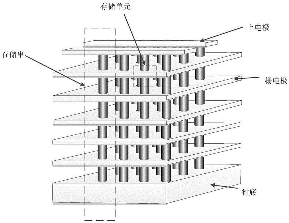
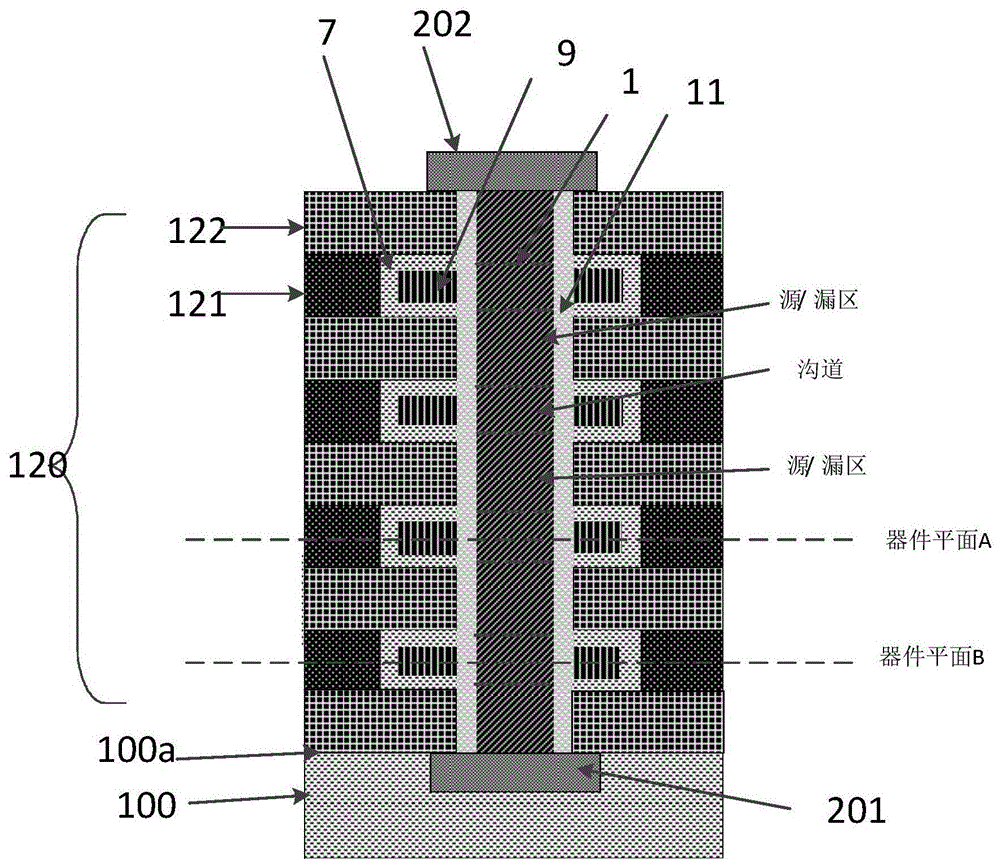
[0064] The invention also provides a method for preparing a nonvolatile three-dimensional semiconductor memory, such as Figure 3-Figure 12 As shown, the preparation process of the NAND storage string specifically includes the following steps:

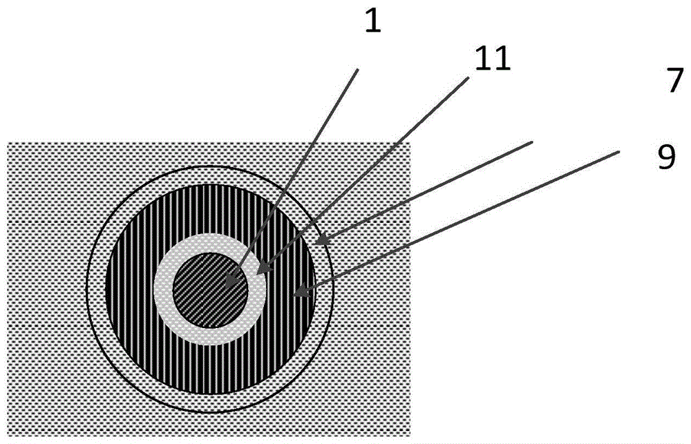
[0065] Step 1: as reference image 3 As shown, a multi-layer film stack structure 120 is deposited on the substrate 100 on which the lower electrodes 201 have been distributed. Then perform deep hole etching in the formed stacked structure to form via holes 80, such as Figure 4 shown.

[0066] Wherein, the control gate electrode 121 and the insulating medium 122 can be deposited on the substrate by any suitable deposition method, such as sputtering, CVD, molecular beam epitaxy (MBE, MOLECULAR BEAM EPITAXY) and the like. The control gate electrode 121, insulating medium 122 may be 6 to 100 nanometers thick. In this embodiment, the control gate electrode 121 can be a conductor (such as metal or metal alloy) or a semiconductor (such ...


PUM


Abstract

The invention discloses a non-volatile three-dimensional semiconductor memory and a preparation method thereof, comprising a plurality of vertical three-dimensional NAND storage strings, each three-dimensional NAND storage string including a horizontal substrate, a cylindrical semiconductor region perpendicular to the substrate, The second electrode and the first electrode respectively located on the top and bottom of the semiconductor region, the tunneling dielectric surrounding the cylindrical semiconductor region, a plurality of discrete charge storage layers are distributed above and below the tunneling dielectric, the tunneling dielectric is wrapped and multiple The blocking dielectric layer of the charge storage layer, the control gate electrode stacked with the insulating layer; the cylindrical semiconductor region includes the source region, the drain region and the channel of a plurality of memory cells. The present invention adopts a floating gate transistor as a storage unit, uses a chalcogenide compound as a channel material, and the storage unit adopts a surrounding gate structure, and the channel region and the source and drain regions use the same material to form a junction-free structure, which well avoids short circuits. ditch effect.

Description

technical field [0001] The invention belongs to the technical field of microelectronic devices, and more specifically relates to a nonvolatile three-dimensional semiconductor memory and a preparation method thereof. Background technique [0002] In order to meet the development of high-efficiency and low-cost microelectronics industry, semiconductor memory devices need to have higher integration density. Regarding semiconductor memory devices, because their integration density is very important in determining product prices, that is, high-density integration is very important. For traditional two-dimensional and planar semiconductor storage devices, because their integration density mainly depends on the unit area occupied by a single storage device, the integration degree is very dependent on the quality of the mask process. However, even if expensive process equipment is continuously used to improve the mask process precision, the increase in integration density is still ...

Claims


Application Information

Patent Timeline
Patent Type & Authority Patents(China)
IPC IPC(8): H01L27/115H01L27/11514
CPCH10B43/27
Inventor 缪向水钱航童浩
Owner HUAZHONG UNIV OF SCI & TECH
Why Eureka
Try Eureka