A Reverse Conduction Insulated Gate Bipolar Transistor

A technology of bipolar transistors and insulated gates, applied to semiconductor devices, electrical components, circuits, etc., can solve problems such as uneven current distribution, device burnout, and current density that cannot be too large, and achieve complete current density distribution and high current density. Uniform distribution, avoiding the effect of voltage rebound phenomenon

Active Publication Date: 2017-06-20
PEKING UNIV SHENZHEN GRADUATE SCHOOL
View PDF2 Cites 0 Cited by
  • Summary
  • Abstract
  • Description
  • Claims
  • Application Information

AI Technical Summary

Problems solved by technology

[0004] However, N-type collectors and P-type collectors need to be made in the back collector area of ​​traditional reverse conduction IGBTs, and patterns need to be made on the back, which reduces the yield of thin IGBTs
In addition, if the ratio of the N region is too small, it may lead to current concentration and uneven current distribution, so the current density that the traditional reverse conduction IGBT can conduct under safe working conditions cannot be too large; if the ratio of the N region is too large, the device There may be a voltage rebound phenomenon during the forward conduction process, such as image 3 As shown, the same voltage value corresponds to multiple current values. When the devices are used in parallel, it is easy for one device to enter the high-current working state first, and the other is still in the low-current and high-resistance state, which may cause the device to be burned.

Method used


Image

  • A Reverse Conduction Insulated Gate Bipolar Transistor
  • A Reverse Conduction Insulated Gate Bipolar Transistor
  • A Reverse Conduction Insulated Gate Bipolar Transistor

Examples


Embodiment 1

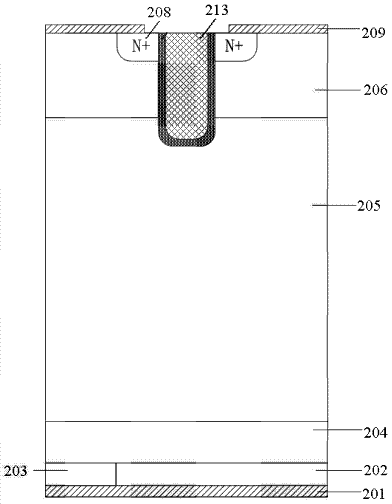
[0023] Such as Figure 4 Shown is a schematic structural diagram of an RC IGBT in a specific embodiment of the present invention. The RCIGBT in this embodiment includes a P-type collector region 02, an N-type tunnel doping region 03, an N-type barrier layer 04, an N-type drift region 05, and a MOS region , the bottom of the P-type collector region is set as the electrode 01 drawn from the collector, and the top of the P-type collector region is an N-type tunnel doping region, an N-type barrier layer, an N-type drift region, and a MOS region; the P-type collector region The electrical region is a degenerate doping region, and the Fermi level enters the valence band; the N-type tunnel doping region is a region where the doping concentration is close to degenerate doping, and the Fermi level is close to the bottom of the conduction band but does not enter the conduction band; The doping concentration of the P-type collector region is higher than that of the N-type tunnel doping r...


PUM


Abstract

A reverse conduction insulated gate bipolar transistor, comprising a collector, a P-type collector region (02), an N-type tunnel doped region (03), an N-type blocking layer (04), an N-type drift region (05), a MOS region and a gate. The P-type collector region (02) is a degenerate doped region, where the Fermi level enters the valence band; the N-type tunnel doped region (03) is a region where the doping concentration is close to degenerate doping, and the Fermi level is close to the bottom of the conduction band but does not enter the conduction band; the doping concentration of the P-type collector region (02) is higher than the doping concentration of the N-type tunnel doped region (03). The transistor realizes reverse conduction by introducing the N-type tunnel doped region (03); thus a back surface does not need an etching process during manufacture. During operation, since the N-type region at the collector end of an ordinary reverse conduction IGBT is not present, the problem of current concentration which arises during forward conduction and reverse conduction of a device is non-existent; the phenomenon of voltage rebound during forward conduction of a device is also non-existent.

Description

technical field [0001] The present application relates to power semiconductor devices, in particular to a reverse conduction insulated gate bipolar transistor. Background technique [0002] Insulated Gate Bipolar Transistor (IGBT, Insulated Gate Bipolar Transistor) is composed of Metal-Oxide-Semiconductor Field-Effect Transistor (MOSFET) and Bipolar Junction Transistor (BJT) ) composed of a class of emerging compound power semiconductor devices, which are mainly used in the medium and high voltage high power range. [0003] In many applications IGBTs work with inductive loads such as figure 1 In the H-bridge structure shown, the AC electrode is used as an inductive load, and four IGBTs are connected in parallel with the reverse diode, that is, IGBT-1, IGBT-2, IGBT-3 and IGBT-4 are respectively connected in parallel with the reverse diode to play a continuous role. The role of flow and protection. In 2004, Japan's Mitsubishi Corporation integrated diodes into IGBTs in a ve...

Claims


Application Information

Patent Timeline
Patent Type & Authority Patents(China)
IPC IPC(8): H01L29/739H01L29/06
CPCH01L29/06H01L29/739
Inventor 孟航李冰华江兴川林信南
Owner PEKING UNIV SHENZHEN GRADUATE SCHOOL
Why Eureka
Try Eureka