v‑sb‑te phase change material system for phase change memory and preparation method thereof
A phase change memory and phase change material technology, which is applied to the V-Sb-Te phase change material system and the field of its preparation, can solve the problem that the performance requirements of the phase change material cannot be met, the thermal stability of the amorphous state is poor, and the crystallization activation energy is small. and other problems, to achieve the best data retention and phase stability, good scalability, and fast phase transition.
- Summary
- Abstract
- Description
- Claims
- Application Information
AI Technical Summary
Problems solved by technology
Method used
Image
Examples
Embodiment 1
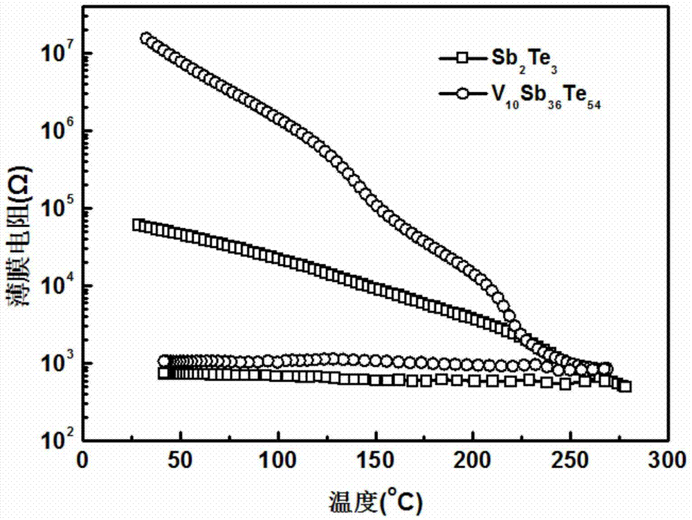
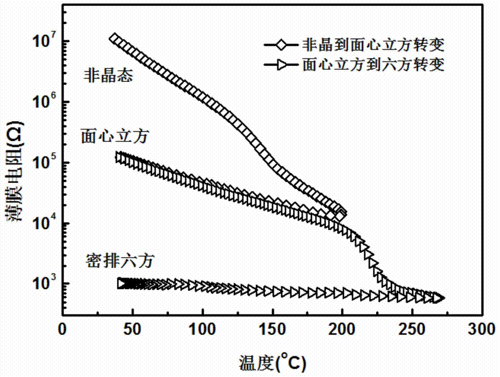
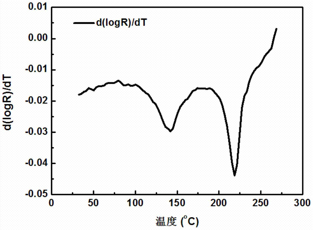
[0023] This embodiment provides a V-Sb-Te phase change material system for phase change memory, wherein the V-Sb-Te phase change material system is formed by doping V on the basis of the Sb-Te phase change material system , whose general chemical formula is V 100-x-y Sb x Te y , wherein, 0.5≤x / y≤4 (where x / y represents the ratio of x to y), and 50≤x+y≤99.99 (where x+y represents the sum of x and y).
[0024] Preferably, at the V 100-x-y Sb x Te y Among them, 1.6≤x / y≤4, wherein, the value range of x is 20≤x≤80, the value range of y is 10≤y≤65, and the atomic percentage of V is not more than 50%. In this embodiment, in the V—Sb—Te phase change material system, the atomic percentage of V is 0.1%˜30%.
[0025] The V-Sb-Te phase-change material system can realize the reversible change of optical reflectivity under the action of laser pulse, and the reversible change of resistivity under the action of electric pulse, so as to realize the function of storing data.
[0026] Thi...
Embodiment 2
[0033] This embodiment provides a V-Sb-Te phase change material for phase change memory, the general chemical formula of the V-Sb-Te phase change material is V 30 Sb 28 Te 42 , and using Sb 2 Te 3 Co-sputtering of alloy target and V elemental target to obtain V 30 Sb 28 Te 42 For thin films, different thicknesses of materials can be controlled by controlling the sputtering time. In this embodiment, sputtering is under 99.999% argon atmosphere, Sb 2 Te 3 The alloy target is sputtered with a DC power supply, and the V target is sputtered with a radio frequency power supply. The sputtering time is 20 minutes, and the obtained V 30 Sb 28 Te 42 The film thickness is about 120nm. where, to obtain V 30 Sb 28 Te 42 Compared with the traditional Sb-Te phase change material, the performance of the thin film is improved in terms of thermal stability and data retention ability.
Embodiment 3
[0035] This embodiment provides a V-Sb-Te phase change material for phase change memory, the general chemical formula of the V-Sb-Te phase change material is V 1 Sb 40 Te 59 , and using Sb 2 Te 3 Co-sputtering of alloy target and V elemental target to obtain V 1 Sb 40 Te 59 For thin films, different thicknesses of materials can be controlled by controlling the sputtering time. In this embodiment, sputtering is under 99.999% argon atmosphere, Sb 2 Te 3 The alloy target is sputtered with a DC power supply, and the V target is sputtered with a radio frequency power supply. The sputtering time is 20 minutes, and the obtained V 1 Sb 40 Te 59 The film thickness is about 120nm. where, to obtain V 1 Sb 40 Te 59 Compared with the traditional Sb-Te phase change material, the performance of the thin film is improved in terms of thermal stability and data retention ability.
PUM
| Property | Measurement | Unit |
|---|---|---|
| thickness | aaaaa | aaaaa |
Abstract
Description
Claims
Application Information


