

Film-forming method and application of n-type in2s3 buffer layer
A film forming method and buffer layer technology, which are applied in coating, metal material coating process, ion implantation plating, etc., can solve the problems such as the influence of the light transmission characteristics of thin films on the performance of solar cells, difficulty in accurately controlling the composition of thin films, etc. The effect of short cycle time, consistent target composition and high deposition rate
- Summary
- Abstract
- Description
- Claims
- Application Information
AI Technical Summary
Problems solved by technology
Method used
Image

Examples
preparation example Construction
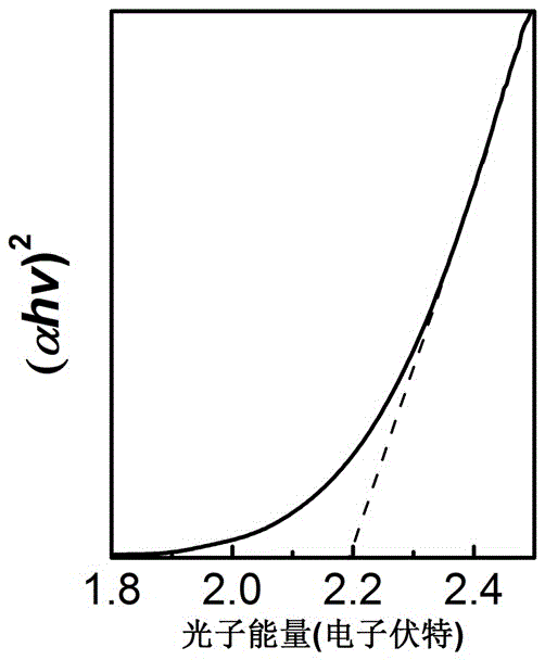
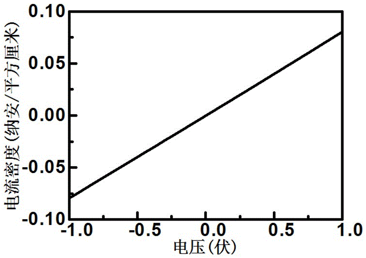
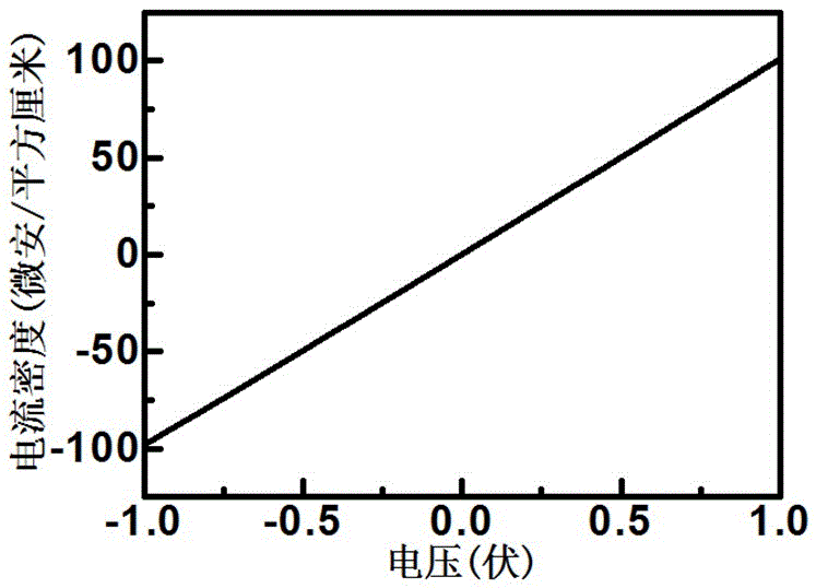
[0055] Adopt preparation n-type In of the present invention 2 S 3 The solar cell that the product that the method for buffer layer obtains is further prepared, this solar cell is made of n-In 2 S 3 The buffer layer 3 of the film and the substrate 1 made of p-Si; the n-In 2 S 3 The buffer layer 3 of the film is β-In 2 S 3 film composition. The top surface of the substrate 1 made of p-Si and the material made of n-In 2 S 3 The bottom surface of the buffer layer 3 of the film is connected; when the material is n-In 2 S 3 The top surface of the buffer layer 3 of the thin film is provided with round electrodes 4 arranged in an array with a thickness of 30-50 nm and made of metal In; the bottom surface of the substrate 1 made of p-Si is provided with a material The bottom electrode layer 2 is metal Ag; the n-In 2 S 3 The resistivity of the buffer layer 3 of the film is 1.00–5.00×10 -3 Ω·cm; the open circuit voltage of the solar cell is 0.29V, the short circuit current i...
Embodiment 1
[0061] Use glass as the substrate, soak it in acetone, ethanol, and deionized water for 8 minutes, respectively, and ultrasonically clean it for 8 minutes, take it out, and dry it in a vacuum oven; 2 S 3 The compound target is fixed on the target holder, the silicon wafer is fixed on the sample holder, the temperature of the vacuum chamber is normal temperature, and the vacuum is pumped to 5×10 -3Below Pa, the rotation speed of the target holder is 5r / min counterclockwise, the rotation speed of the sample holder is 5r / min clockwise, the laser wavelength is 248nm, the pulse width is 25ns, the laser energy is 154mJ, the laser frequency is 5Hz, and the coating time is 30min. During annealing, pre-evacuate the rapid annealing furnace to 1Pa, then pass Ar gas to atmospheric pressure, then evacuate, repeatedly evacuate and inflate twice, and then continuously pass Ar gas to keep the pressure at about 0.04MPa. The temperature was raised to 300°C at a speed of s, maintained at this t...
Embodiment 2
[0064] A p-type silicon wafer was used as the substrate 1, soaked in acetone, ethanol, and deionized water for 8 minutes, respectively, and ultrasonically cleaned for 8 minutes, and then dried in a vacuum oven after being taken out; 2 S 3 The compound target is fixed on the target holder, the silicon wafer is fixed on the sample holder, the temperature of the vacuum chamber is normal temperature, and the vacuum is pumped to 5×10 -3 Below Pa, the rotation speed of the target holder is 5r / min counterclockwise, the rotation speed of the sample holder is 5r / min clockwise, the laser wavelength is 248nm, the pulse width is 25ns, the laser energy is 174mJ, the laser frequency is 5Hz, and the coating time is 30min. During annealing, the rapid annealing furnace is pre-evacuated to below 1Pa, and Ar gas is introduced to atmospheric pressure, and the vacuum and inflated are repeated twice, and then Ar gas is introduced to keep the pressure at about 0.04MPa, and the temperature is raised ...
PUM
| Property | Measurement | Unit |
|---|---|---|
| diameter | aaaaa | aaaaa |
| thickness | aaaaa | aaaaa |
| electrical resistivity | aaaaa | aaaaa |
Abstract
Description
Claims
Application Information