Three-dimensional figure detecting device and measuring method

A technology of three-dimensional graphics and detection devices, which is applied to measurement devices, optical devices, instruments, etc., can solve problems such as low utilization of light energy, save equipment costs, improve detection efficiency, and simplify solution methods.

Active Publication Date: 2015-01-14
SHANGHAI MICRO ELECTRONICS EQUIP (GRP) CO LTD
View PDF9 Cites 24 Cited by
  • Summary
  • Abstract
  • Description
  • Claims
  • Application Information

AI Technical Summary

Problems solved by technology

[0009] The present invention provides a three-dimensional graphic detection device and measurement method to overcome the problems of the prior art that require a high-resolution spectrometer, low utilization rate of light energy, simulation modeling required for solution, and only one TSV can be detected at a time

Method used


Image

  • Three-dimensional figure detecting device and measuring method
  • Three-dimensional figure detecting device and measuring method
  • Three-dimensional figure detecting device and measuring method

Examples


Embodiment 1

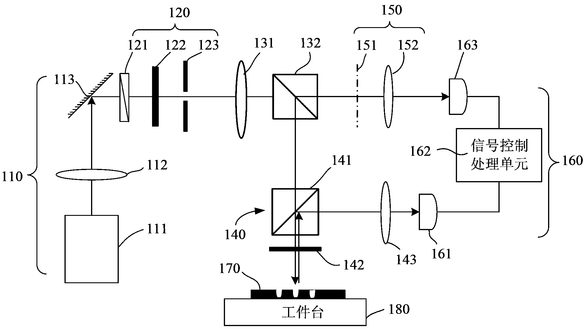
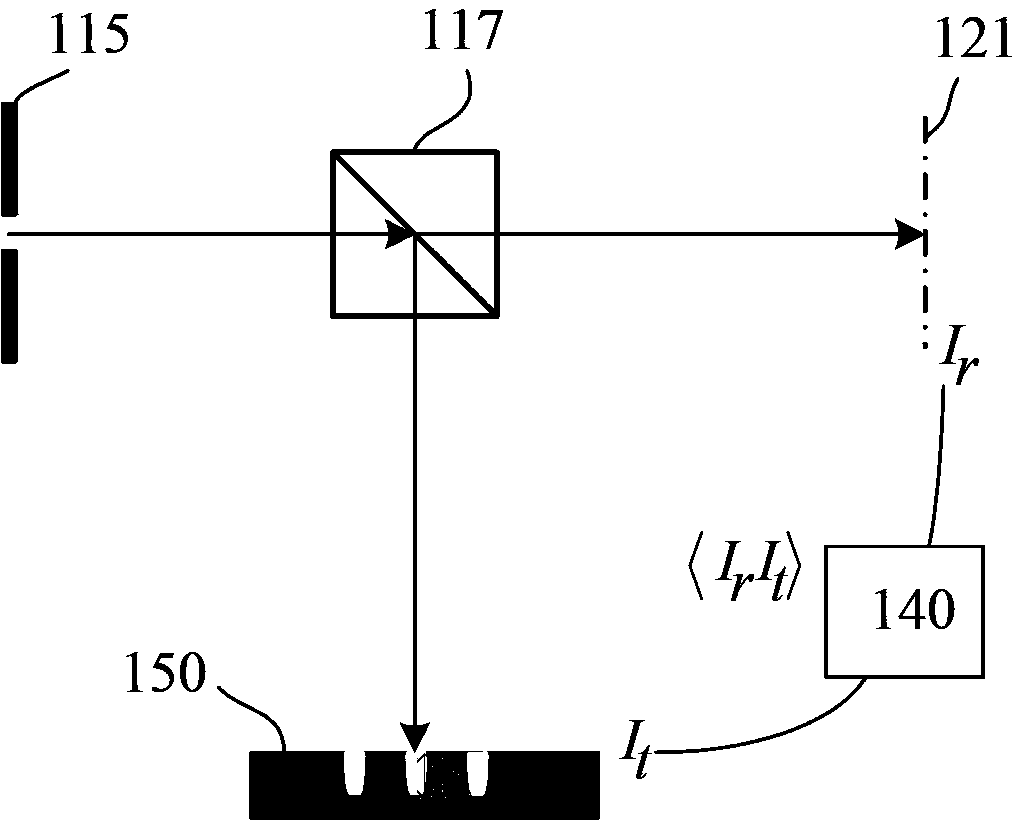
[0066] Please refer to figure 1 , the three-dimensional pattern detection device provided in this embodiment is used to detect the sample 150 to be tested, which includes:

[0067] an illumination projection module 110, configured to generate a detection beam and a reference beam, and project the detection beam onto the surface of the sample to be measured 150;

[0068] The reference imaging module 120 includes a reference plane 121, the reference imaging module 120 is used to collect the reference beam projected onto the reference plane 121 to generate a reference light intensity distribution signal;

[0069] The detection imaging module 130 is used to collect the reflected and diffracted light on the surface of the sample 150 to be tested to generate a detection light intensity distribution signal; and

[0070] The control processing module 140 is configured to perform an intensity correlation operation on the light intensity distribution signal of the probe light and the l...

Embodiment 2

[0104] The difference between this embodiment and Embodiment 1 is that the illumination light sources used in this embodiment are different, and the corresponding optical modulation components are also different.

[0105] Please refer to Figure 8 , in this embodiment, the illumination light source 210 uses multiple lasers 211 with different wavelengths, for example, the wavelengths are λ 1 , lambda 2 , lambda 3 lasers 211, and the laser beams generated by the multiple lasers 211 enter the optical modulation component 220 through a single-mode polarization-maintaining fiber 212 and a multiplexer 213. Further, the optical modulation component 220 includes a beam expander 221 , a rotating glass 222 , a polarizer 223 and a lens 224 sequentially arranged along the light propagation direction for beam shaping of the light emitted by the illumination source 210 . Preferably, the rotation of the rotating glass 222 is controlled by a motor 225 .

[0106] Specifically, the laser be...

Embodiment 3

[0111] The lighting projection module of this embodiment is the same as that of Embodiment 2, and the common difference between Embodiment 1 and Embodiment 2 is that the reference imaging module in this embodiment is a virtual module, therefore, there is no need to use a separate imaging module in this embodiment. Beamer, control processing module and embodiment 1 and 2 are also different.

[0112] Please refer to Figure 9 , in this embodiment, the illumination projection module also includes an illumination light source 310, an optical modulation assembly 320, a variable diaphragm 330, and a reflector 340 arranged in sequence along the light propagation direction, wherein the structure of the illumination light source 310 is the same as that in Embodiment 2, Both adopt a plurality of lasers 311 with different wavelengths as the light source of the three-dimensional pattern detection device, and the optical modulation component 320 includes a beam expander 321, a spatial ligh...


PUM


Abstract

The invention discloses a three-dimensional figure probe device and measuring method. The device comprises an illumination projecting module, a reference imaging module, a probe imaging module and a control processing module. The illumination projecting module is used for generating probe beams and reference beams, and projecting the probe beams to the surface of a sample to be detected. The reference imaging module comprises a reference plane and is used for collecting the reference beams projected to the reference plane so as to generate reference light intensity distribution signals. The probe imaging module is used for probe reflected light and diffraction light on the surface of the sample to be detected so as to generate probe light intensity distribution signals. The control processing module is used for carrying out the intensity correlation operation on the probe light intensity distribution signals and the reference light intensity distribution signals, and surface appearance parameters of the sample to be detected are obtained. By means of a traditional imaging probe mode, the zero-level reflected light and various levels of diffraction light of a silicon wafer to be detected are collected, space light filtering is not needed, and the light use efficiency is improved. The illumination of a large visual field is achieved, probe light spots can cover a plurality of surface appearances, and the detecting efficiency is improved.

Description

technical field [0001] The invention relates to the field of semiconductor manufacturing, in particular to a three-dimensional pattern detection device and a measurement method. Background technique [0002] With the development of semiconductor manufacturing technology and the continuous improvement of chip integration, it has become increasingly difficult to further reduce the feature size of devices in order to satisfy Moore's law. In order to overcome the above difficulties, a vertical packaging technology based on through-silicon vias (TSV, through Silicon Via) has been gradually developed, which can obtain semiconductor devices with higher integration. TSV is a 3D packaging technology that realizes the interconnection between chips by making vertical conduction between chips and chips, wafers and wafers. The density of chips stacked in three dimensions is higher, the integration per unit area is higher, and the performance of chip speed and low power consumption is gr...

Claims


Application Information

Patent Timeline
Patent Type & Authority Applications(China)
IPC IPC(8): G01B11/24
Inventor 张鹏黎王帆
Owner SHANGHAI MICRO ELECTRONICS EQUIP (GRP) CO LTD
Why Eureka
Try Eureka