Feed network for reducing mutual coupling between antenna array units
A technology of antenna unit and antenna array, applied in the direction of antenna, electrical components, etc., can solve problems such as difficult implementation, difficult processing, huge difference in Q value and efficiency of different modes, and achieve the effect of avoiding energy loss and simple structure
- Summary
- Abstract
- Description
- Claims
- Application Information
AI Technical Summary
Problems solved by technology
Method used
Image
Examples
Embodiment 1
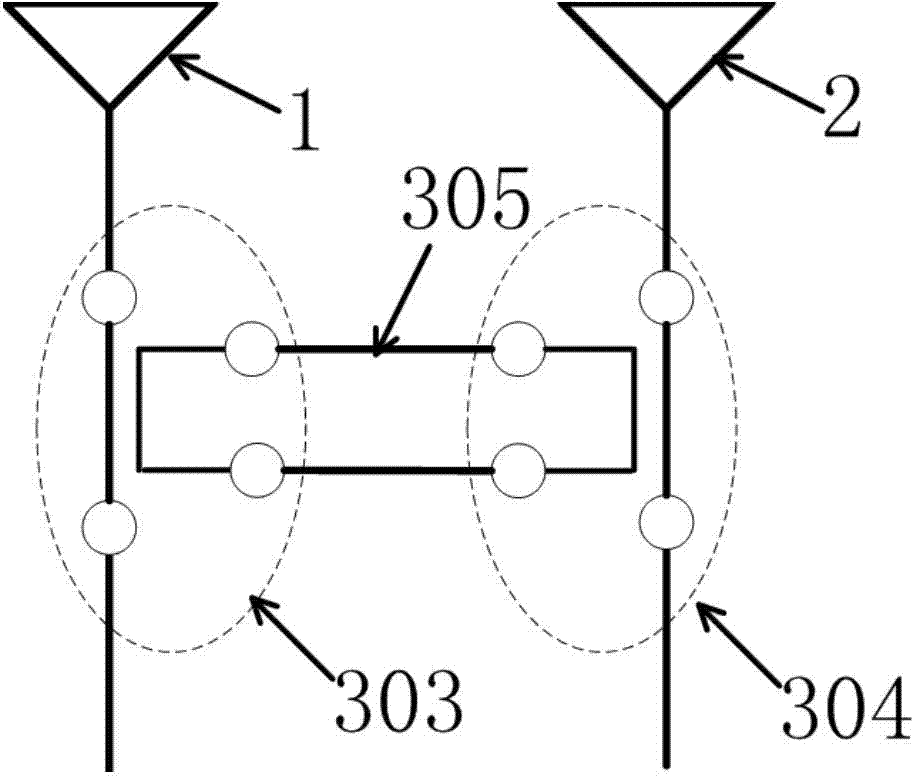
[0027] This embodiment adopts an array structure of two antenna elements, which adopts the feeding network of the present invention such as image 3 As shown, the couplers of the coupling network are two-wire four-port coupled microstrip line couplers 303 and 304 , and the corresponding ports of the coupler 303 and the coupler 304 are connected through phase-adjusted transmission lines 305 .
[0028] In this embodiment, the specific structure of the antenna array using the feeding network of the present invention is as follows: Figure 4 As shown, the antenna unit uses a microstrip antenna, and the coupling network uses a two-wire coupled microstrip line coupler. The overall structure of the array is divided into three layers, as shown in the section Figure 4 As shown in (b): the uppermost layer is the antenna layer, including a 3mm thick dielectric layer 122 (relative permittivity 2.2) and a microstrip patch 123; the middle layer is used as the ground, and the material is a...
Embodiment 2
[0033] Figure 9 It is a schematic diagram of the 16-element array structure and the feeding network used in this embodiment. The dotted box 162 is a schematic diagram of a three-line coupled microstrip line coupler, which is used as a coupler structure in the coupling network in this embodiment.
[0034] Figure 10 It is a specific structural diagram of the array of antennas and its feed network used in this embodiment. The antenna unit adopts a microstrip antenna, and the couplers adopt a microstrip two-wire directional coupler. The overall structure of the array is divided into three layers, as shown in the section Figure 10 (b) shown. For clarity, section Figure 10 (b) Only intercept the middle part of the array, but without loss of generality: the uppermost layer is the antenna layer, including a 3mm thick dielectric layer 172 (relative permittivity 2.2) and a microstrip patch 173; the middle layer is used as the ground, and the material is 5mm aluminum plate 171;...
PUM
 Abstract
Description
Claims
Application Information


