PNIN type InGaAs infrared detector
A technology of infrared detectors and detectors, applied in semiconductor devices, electrical components, circuits, etc., can solve problems such as incompatibility, achieve good versatility, inhibit transportation, and achieve the effect of performance
- Summary
- Abstract
- Description
- Claims
- Application Information
AI Technical Summary
Problems solved by technology
Method used
Image
Examples
Embodiment 1
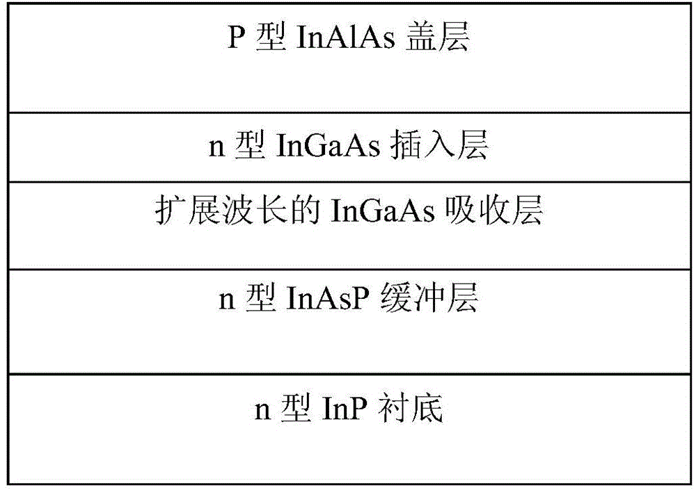
[0021] Combine figure 1 To illustrate this embodiment, a PNIN-type InGaAs infrared detector with a cut-off wavelength of 2.6 μm is structured as follows: a thickness of about 1 μm and a doping concentration of 2×10 are sequentially grown on an n-type InP substrate. 18 cm -3 N-type InAs 0.60 P 0.40 Buffer layer, continue to grow with a thickness of 3μm and a doping concentration of 8×10 16 cm -3 N-type In 0.82 Ga 0.18 As absorption layer, the thickness of the re-growth is 100nm, and the doping concentration is 5×10 17 cm -3 N-type In 0.82 Ga 0.18 As insertion layer, the final growth thickness is 1μm, and the doping concentration is 2×10 18 cm -3 P-type In 0.82 Al 0.18 As cover layer, forming the PNIN detector structure.
[0022] In this embodiment, a MOCVD system is first used to grow Si-doped InAs on an n-type InP substrate using a two-step method. 0.60 P 0.40 Buffer layer, first grow a layer of InAs about 1μm at a temperature of 450℃ 0.60 P 0.40 , And then raise the temperature to...
Embodiment 2
[0024] A PNIN-type InGaAs infrared detector with a cut-off wavelength of 2.6μm. Its structure is: sequentially grown on an n-type GaAs substrate with a thickness of about 1μm and a doping concentration of 2×10 18 cm -3 N-type InAs 0.60 P 0.40 Buffer layer, continue to grow with a thickness of 3μm and a doping concentration of 8×10 16 cm -3 N-type In 0.82 Ga 0.18 As absorption layer, the thickness of the re-growth is 150nm, the doping concentration is 5×10 17 cm -3 N-type In 0.82 Ga 0.18 As insertion layer, the final growth thickness is 1μm, and the doping concentration is 2×10 18 cm -3 P-type In 0.82 Al 0.18 As cover layer, forming the PNIN detector structure.
[0025] In this embodiment, a MOCVD system is used to grow Si-doped InAs on an n-type GaAs substrate using a two-step method. 0.60 P 0.40 Buffer layer, first grow a layer of InAs about 1μm at a temperature of 450℃ 0.60 P 0.40 , And then raise the temperature to 580℃, the buffer layer InAs 0.60 P 0.40 Annealing recrystallizati...
Embodiment 3
[0027] A PNIN-type InGaAs infrared detector with a cut-off wavelength of 2.6μm. Its structure is: sequentially grown on an n-type InP substrate with a thickness of about 1μm and a doping concentration of 2×10 18 cm -3 N-type InAs 0.60 P 0.40 Buffer layer, continue to grow with a thickness of 3μm and a doping concentration of 8×10 16 cm -3 N-type In 0.82 Ga 0.18 As absorption layer, the thickness of re-growth is 50nm, the doping concentration is 5×10 17 cm -3 N-type In 0.82 Ga 0.18 As insertion layer, the final growth thickness is 1μm, and the doping concentration is 2×10 18 cm -3 P-type In 0.82 Al 0.18 As cover layer, forming the PNIN detector structure.
[0028] In this embodiment, a MOCVD system is first used to grow Si-doped InAs on an n-type InP substrate using a two-step method. 0.60 P 0.40 Buffer layer, first grow a layer of InAs about 1μm at a temperature of 450℃ 0.60 P 0.40 , And then raise the temperature to 580℃, the buffer layer InAs 0.60 P 0.40 Annealing recrystallizatio...
PUM
 Abstract
Description
Claims
Application Information
