A method for manufacturing a multi-step microlens and a method for manufacturing a step of an optical element

A production method and technology of optical components, applied in the direction of optical components, optics, lenses, etc., can solve problems such as alignment, photolithography, etching, etc., and achieve the effect of meeting high-precision requirements, reducing difficulty, and reducing process steps

Active Publication Date: 2016-05-04
中航凯迈上海红外科技有限公司
View PDF5 Cites 0 Cited by
  • Summary
  • Abstract
  • Description
  • Claims
  • Application Information

AI Technical Summary

Problems solved by technology

[0007] The purpose of the present invention is to provide a method for making any multi-step microlens by corroding the shielding layer, so as to solve the problems of alignment, photolithography and etching caused by the mask plate in the traditional overlay method

Method used


Image

  • A method for manufacturing a multi-step microlens and a method for manufacturing a step of an optical element
  • A method for manufacturing a multi-step microlens and a method for manufacturing a step of an optical element
  • A method for manufacturing a multi-step microlens and a method for manufacturing a step of an optical element

Examples


Embodiment 1

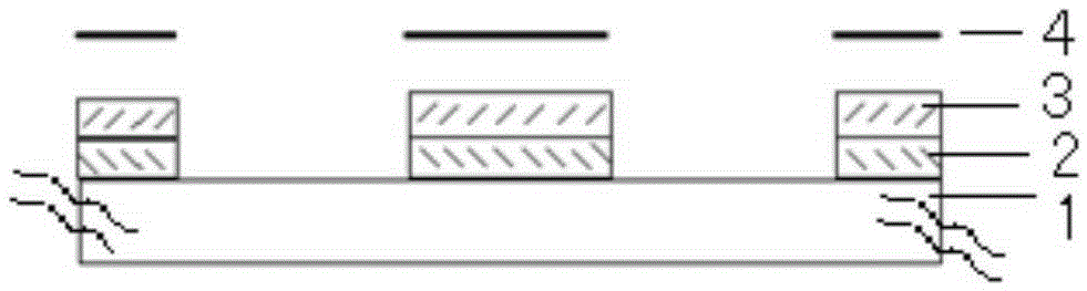
[0025] When using a multi-step microlens manufacturing method of the present invention to manufacture a quartz-based diffractive microlens array, the specific steps are as shown in the figure:

[0026] 1) Sputtering a Cr metal layer on the quartz substrate 1 with a magnetron sputtering table as the shielding layer 2;

[0027] 2) Spin-coat positive photoresist AZ1500 on the metal layer 2; use the mask plate 4 to expose, carry out photolithography development, and make a pattern as the etching mask layer 3; use Cr etching solution to etch out the outline as the innermost ring The shielding layer with the belt is used as a mask;

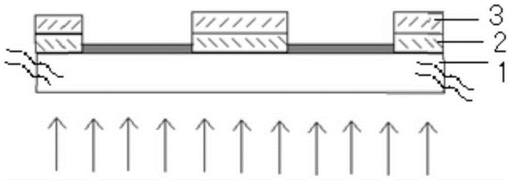
[0028] 3) spin-coating negative photoresist 5; exposing and developing on the back of the substrate 1, and the obtained negative photoresist 5 is used as an etching mask as a protective layer;

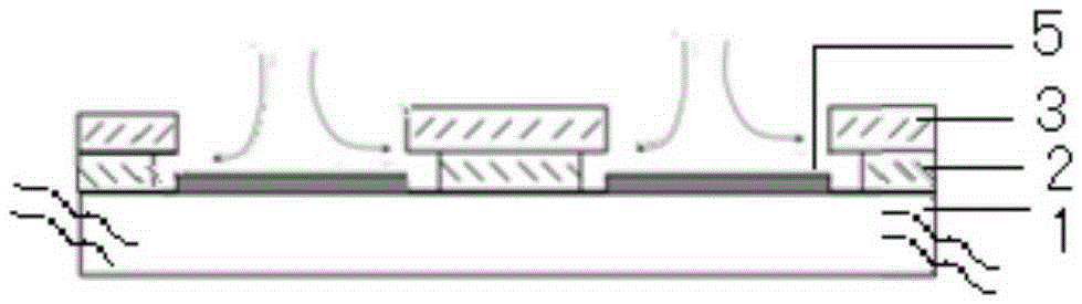
[0029] 4) Laterally corrode the shielding layer Cr metal layer 1 in 1), and the corrosion amount is the width of the second step;

[0030] 5) Remove the posit...

Embodiment 2

[0041] The invention also provides a method for manufacturing optical element steps, which is used for manufacturing optical elements with two layers of steps. Specific steps are as follows:

[0042] 1) Sputtering a Cr metal layer 2 on a quartz substrate 1 with a magnetron sputtering table as a shielding layer;

[0043] 2) Spin-coat positive photoresist AZ1500 on the metal layer 1; use the mask plate 4 to expose, carry out photolithography development, and make a pattern as the etching mask layer 3; use Cr etching solution to etch out the outline as the innermost ring The shielding layer with the belt is used as a mask;

[0044] 3) Spin-coating negative photoresist 5; exposing and developing on the back of the substrate, the obtained negative photoresist 5 is used as an etching mask as a protective layer;

[0045] 4) Laterally corrode the shielding layer Cr metal layer 2 in 1), and the corrosion amount is the width of the second step;

[0046] 5) Remove the positive photore...


PUM


Abstract

The invention relates to a multi-step micro-lens production method and an optical element step production method. According to the method, an innermost layer ring belt of a micro-lens is formed by carrying out only one mask lithography; through negative photoresist back surface exposure development, a mask layer is obtained; pattern of a substrate is formed through corrosion, back surface exposure development, and etching; and ring belt patterns are obtained from the inside out in sequence by carrying out circulation. The invention also provides the optical element step production method. Therefore, unavoidable errors in the processes of mask plate alignment, lithography and etching and the like of the production of the micro-lens produced with the conventional overlay method are fundamentally avoided, thereby reducing process steps in the manufacturing process, reducing difficulty, meeting high-precision requirement in the micro-lens production process, and effectively guaranteeing and improving optical performances of micro-lens diffraction benefit and the like.

Description

technical field [0001] The invention relates to a method for manufacturing a multi-step micro-lens and a method for manufacturing a step of an optical element, and belongs to the field of a photoelectric device manufacturing process method and micro-optics technology. Background technique [0002] The microlens array is an array composed of a series of tiny lenses with diameters of millimeters and micrometers in a certain arrangement. Micro-lenses and micro-lens arrays produced by micro-optical technology have become a new direction of scientific research and development due to their advantages of small size, light weight, easy integration, and arraying. [0003] The diffractive microlens is designed according to the principle of Fresnel zone plate, making ring-shaped steps, each ring-shaped step is centered on the optical axis, and each ring is equivalent to an independent refraction surface. It can make the incident light converge to the same focal point. The more steps, ...

Claims


Application Information

Patent Timeline
Patent Type & Authority Patents(China)
IPC IPC(8): G02B3/00G02B27/44G03F7/00
CPCG02B3/0012G02B27/44
Inventor 侯治锦司俊杰韩德宽陈洪许吕衍秋丁嘉欣张向锋姚官生王理文杨雪峰耿东锋
Owner 中航凯迈上海红外科技有限公司
Why Eureka
Try Eureka