Subwavelength plasmonic microcavity light coupling structure for promoting photoelectric detector response
A photodetector and plasmon technology, which is applied in the direction of electrical components, circuits, semiconductor devices, etc., can solve the problem of low utilization rate of incident photons, achieve high enhancement ability, increase response rate, and improve the effect of response rate
- Summary
- Abstract
- Description
- Claims
- Application Information
AI Technical Summary
Problems solved by technology
Method used
Image
Examples
Embodiment 1
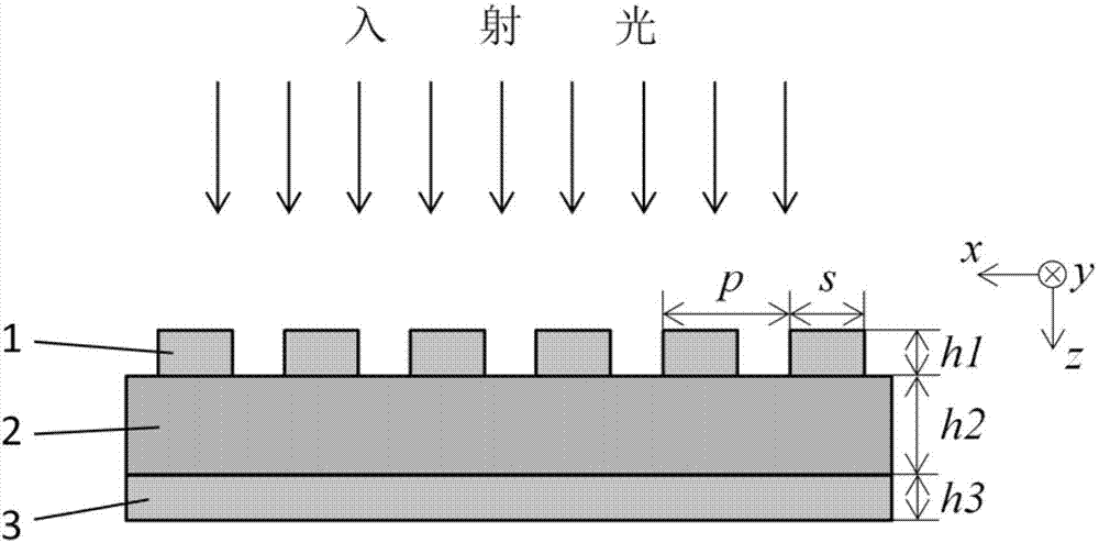
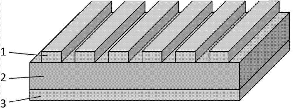
[0029] Embodiment 1: The upper metal is a one-dimensional grating, the line width s is 5.5 microns, the period p is 9.6 microns, and the thickness of the viscous titanium metal is 20 nanometers.
Embodiment 2
[0030] Embodiment 2: The upper metal layer is a one-dimensional grating, and the line width s is taken as 1.36 microns, which is one-tenth of the detection wavelength. The period p is taken as 2.6 microns, which satisfies the condition of being greater than the line width s. The sticky metal titanium is 5 nanometers thick.
Embodiment 3
[0031] Embodiment 3: The upper metal layer is a one-dimensional grating, and the line width s is taken as 13.6 microns, which is ten tenths of the detection wavelength. The period p is taken as 40 microns, which is thirty-tenths of the detection wavelength. The viscous titanium metal is 30 nanometers thick.
PUM
| Property | Measurement | Unit |
|---|---|---|
| Thickness | aaaaa | aaaaa |
| Thickness | aaaaa | aaaaa |
Abstract
Description
Claims
Application Information


