Graphene double-junction solar battery and preparation method thereof
A technology of solar cells and graphene, applied in circuits, photovoltaic power generation, electrical components, etc., can solve problems such as reducing battery open circuit voltage and short circuit current, affecting battery photoelectric conversion efficiency, etc., to increase short circuit current and open circuit voltage, and improve photoelectricity Effect of conversion efficiency and efficiency improvement
- Summary
- Abstract
- Description
- Claims
- Application Information
AI Technical Summary
Problems solved by technology
Method used
Image
Examples
Embodiment 1
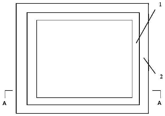
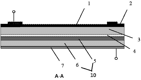
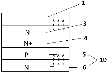
[0026] See figure 1 and figure 2 , first at a doping concentration of 10 15 / cm 3 One side of the N-type monocrystalline silicon wafer 3 is prepared by plasma vapor phase chemical deposition with a doping concentration of 10 19 / cm 3 N-type polysilicon film 4 with a thickness of 50nm; then sequentially deposited on its surface with a doping concentration of 10 15 / cm 3 The P-type polysilicon film 5 and the N-type polysilicon film 6 both have a thickness of 30um. The P-type polysilicon film 5 and the N-type polysilicon film 6 form a PN junction 10 . Prepare a 100nm silicon dioxide layer 2 on the other side of the N-type single crystal silicon wafer 3, and then use a spraying process on the surface of the silicon dioxide layer 2 and the surface of the single crystal silicon 3 exposed by the through hole of the silicon dioxide layer 2 A 10nm graphene film 1 is prepared, and the graphene film 1 is combined with an N-type single crystal silicon wafer 3 after drying. Then a...
Embodiment 2
[0028] Please combine embodiment 1, at first the doping concentration is 10 14 / cm 3 One side of the P-type single crystal silicon wafer 3 is sequentially prepared with a doping concentration of 10 by plasma vapor chemical deposition method. 19 / cm 3 P-type polysilicon thin film 4 with a thickness of 150nm; then sequentially deposited on its surface with a doping concentration of 10 14 / cm 3 The N-type polysilicon film 5 and the P-type polysilicon film 6 both have a thickness of 50um. The N-type polysilicon film 5 and the P-type polysilicon film 6 form a PN junction 10 . Prepare a 100nm silicon dioxide layer 2 on the other side of the P-type monocrystalline silicon wafer 3, and then use a spraying process on the surface of the silicon dioxide layer 2 and the surface of the monocrystalline silicon 3 exposed by the through hole of the silicon dioxide layer 2 A 10nm graphene film 1 is prepared, and the graphene film 1 is combined with a P-type single crystal silicon wafer 3 ...
Embodiment 3
[0030] Please combine embodiment 1, at first the doping concentration is 10 14 / cm 3 One side of the P-type single crystal silicon wafer 3 is sequentially prepared with a doping concentration of 10 by plasma vapor chemical deposition method. 20 / cm 3 The N-type polysilicon film and the doping concentration is 10 20 / cm 3 The P-type polysilicon thin film constitutes the tunnel junction 4 with a thickness of 100nm; 14 / cm 3The N-type polysilicon film 5 and the P-type polysilicon film 6 both have a thickness of 50um. The N-type polysilicon film 5 and the P-type polysilicon film 6 form a PN junction 10 . Prepare a 100nm silicon dioxide layer 2 on the other side of the P-type monocrystalline silicon wafer 3, and then use a spraying process on the surface of the silicon dioxide layer 2 and the surface of the monocrystalline silicon 3 exposed by the through hole of the silicon dioxide layer 2 A 10nm graphene film 1 is prepared, and the graphene film 1 is combined with a P-type...
PUM
| Property | Measurement | Unit |
|---|---|---|
| Doping concentration | aaaaa | aaaaa |
| Thickness | aaaaa | aaaaa |
| Thickness | aaaaa | aaaaa |
Abstract
Description
Claims
Application Information


