

Electronically Controlled Liquid Crystal Laser Shaping Chip Based on Wavefront Adjustment
A laser shaping and liquid crystal technology, applied in optics, nonlinear optics, instruments, etc., can solve the problems of long state transition time, difficulty in integrating into space and drive control, large volume and quality, etc., and achieve flexible electric drive control mode, drive The effect of flexible control mode and high control precision
- Summary
- Abstract
- Description
- Claims
- Application Information
AI Technical Summary
Problems solved by technology
Method used
Image

Examples
Embodiment Construction
[0020] In order to make the object, technical solution and advantages of the present invention clearer, the present invention will be further described in detail below in conjunction with the accompanying drawings and embodiments. It should be understood that the specific embodiments described here are only used to explain the present invention, not to limit the present invention. In addition, the technical features involved in the various embodiments of the present invention described below can be combined with each other as long as they do not constitute a conflict with each other.
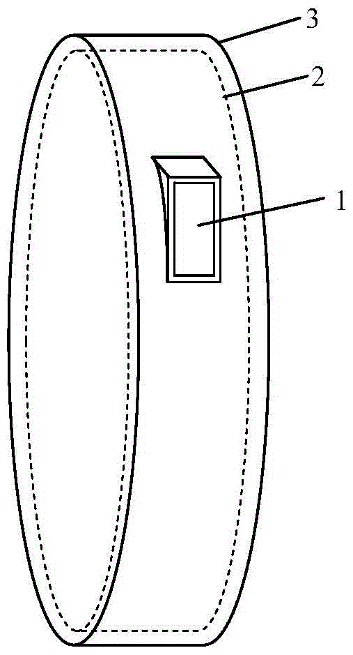
[0021] Such as figure 1 As shown, the electronically controlled liquid crystal laser shaping chip based on wavefront adjustment according to the embodiment of the present invention includes a chip housing 3 and a cylindrical liquid crystal phase modulation structure 2 . The liquid crystal phase modulation structure 2 is packaged in the chip case 3 and fixedly connected with the chip case 3 , an...
PUM
 Abstract
Description
Claims
Application Information