Tunneling field effect transistor inhibiting output non-linear opening and preparing method of tunneling field effect transistor

A tunneling field effect and transistor technology, which is applied in semiconductor devices, semiconductor/solid-state device manufacturing, electrical components, etc., can solve the problems of low on-state current, failure to meet system integration application requirements, and low band tunneling efficiency. Achieving a steep sub-threshold slope, improving the output characteristics of the device, and suppressing the nonlinear turn-on phenomenon

Active Publication Date: 2015-02-11
PEKING UNIV
View PDF5 Cites 9 Cited by
  • Summary
  • Abstract
  • Description
  • Claims
  • Application Information

AI Technical Summary

Problems solved by technology

[0003] However, due to the low efficiency of semiconductor band-band tunneling, the on-state current of TFET is lower than that of traditional MOSFETs, which cannot meet the requirements of system integration applications.

Method used


Image

  • Tunneling field effect transistor inhibiting output non-linear opening and preparing method of tunneling field effect transistor
  • Tunneling field effect transistor inhibiting output non-linear opening and preparing method of tunneling field effect transistor
  • Tunneling field effect transistor inhibiting output non-linear opening and preparing method of tunneling field effect transistor

Examples


Embodiment Construction

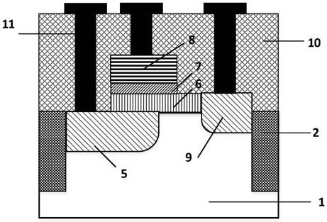
[0043] The implementation method of the tunneling field effect transistor for suppressing output nonlinear turn-on according to the present invention will be further described through specific embodiments below in conjunction with the accompanying drawings.

[0044] The specific implementation steps are as Figure 1-Figure 7 Shown: (This example takes N-type devices as an example, and P-type devices can be deduced by analogy)

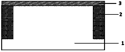
[0045] 1. The substrate doping concentration is lightly doped (about 1E13cm -3 -1E15cm -3 ), a layer of silicon dioxide 3 is initially thermally oxidized on a Si substrate 1 with a crystal orientation of , with a thickness of about 10 nm, and a layer of silicon nitride (Si 3 N 4 ), with a thickness of about 100nm, and then use shallow trench isolation technology to make STI isolation 2 in the active area, and then perform CMP, such as figure 2 shown;

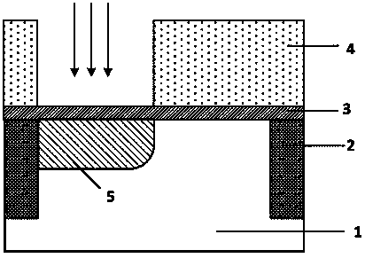
[0046] 2. Expose the tunneling source region 5 by photolithography, and use the photoresist 4 as...


PUM


Abstract

The invention provides a tunneling field effect transistor inhibiting output non-linear opening. The tunneling field effect transistor comprises a tunneling source region, a channel region, a drain region, a semiconductor substrate region, a gate dielectric layer and a control gate, wherein the gate dielectric layer is positioned above the channel region, the control gate is positioned above the gate dielectric layer, the channel region is positioned above the channel source region, in addition, the position of the channel region is partially overlapped with the tunneling source region, a tunneling junction is formed at the interface part of the channel region and the tunneling source region, the drain region is parallel to the channel region and is positioned at the other side of the channel region, the control gate is positioned above the overlapping part of the channel region and the tunneling source region, a control-gate-free region is arranged in the channel region near the drain region, and in addition, the channel region adopts semiconductor materials with the energy state density being lower than 1E18cm<-3>. The tunneling field effect transistor has the advantages that the nonlinear opening phenomenon in the device output characteristics can be effectively inhabited, and in addition, the steeper and straighter sub-threshold slope is maintained.

Description

technical field [0001] The invention belongs to the field of field-effect transistor logic devices of CMOS ultra-large-scale integrated circuits (ULSI), and in particular relates to a tunneling field-effect transistor capable of suppressing output nonlinear turn-on and a preparation method thereof. Background technique [0002] Since the birth of integrated circuits, microelectronics integration technology has been developing continuously in accordance with "Moore's Law", and the size of semiconductor devices has been continuously reduced. As semiconductor devices enter the deep submicron range, traditional MOSFET devices are limited by the conduction mechanism of self-diffusion drift, and the subthreshold slope is limited by the thermoelectric potential kT / q, which cannot be reduced synchronously with the reduction of device size. As a result, the reduction of leakage current of MOSFET devices cannot meet the requirements of device size reduction, the energy consumption of ...

Claims


Application Information

Patent Timeline
Patent Type & Authority Applications(China)
IPC IPC(8): H01L29/739H01L21/331
CPCH01L29/66325H01L29/7391
Inventor 黄如吴春蕾黄芊芊王阳元
Owner PEKING UNIV
Why Eureka
Try Eureka