Scan test latch macrocell and scan test method

A technology of scan test and latch, which is applied in the field of scan test macrocell and scan test, can solve the problems of insufficient fault coverage and design complexity, and achieve the goal of reducing test escape rate, low degree of automation and fast operation speed Effect

Active Publication Date: 2015-02-25
BEIJING MXTRONICS CORP +1
View PDF7 Cites 13 Cited by
  • Summary
  • Abstract
  • Description
  • Claims
  • Application Information

AI Technical Summary

Problems solved by technology

[0008] The problem solved by the technology of the present invention is: to overcome the deficiencies in the fault coverage and design complexity of the existing latch-based testability design method, and propose a scan test latch macrocell and a scan test method , the invention is aimed at the Mux-Scan scan test of the latch unit, which can not only use the existing scan test methodology and EDA tools for the D flip-flop unit, simplify the design process, but also ensure a very high fault coverage

Method used


Image

  • Scan test latch macrocell and scan test method
  • Scan test latch macrocell and scan test method
  • Scan test latch macrocell and scan test method

Examples


Embodiment Construction

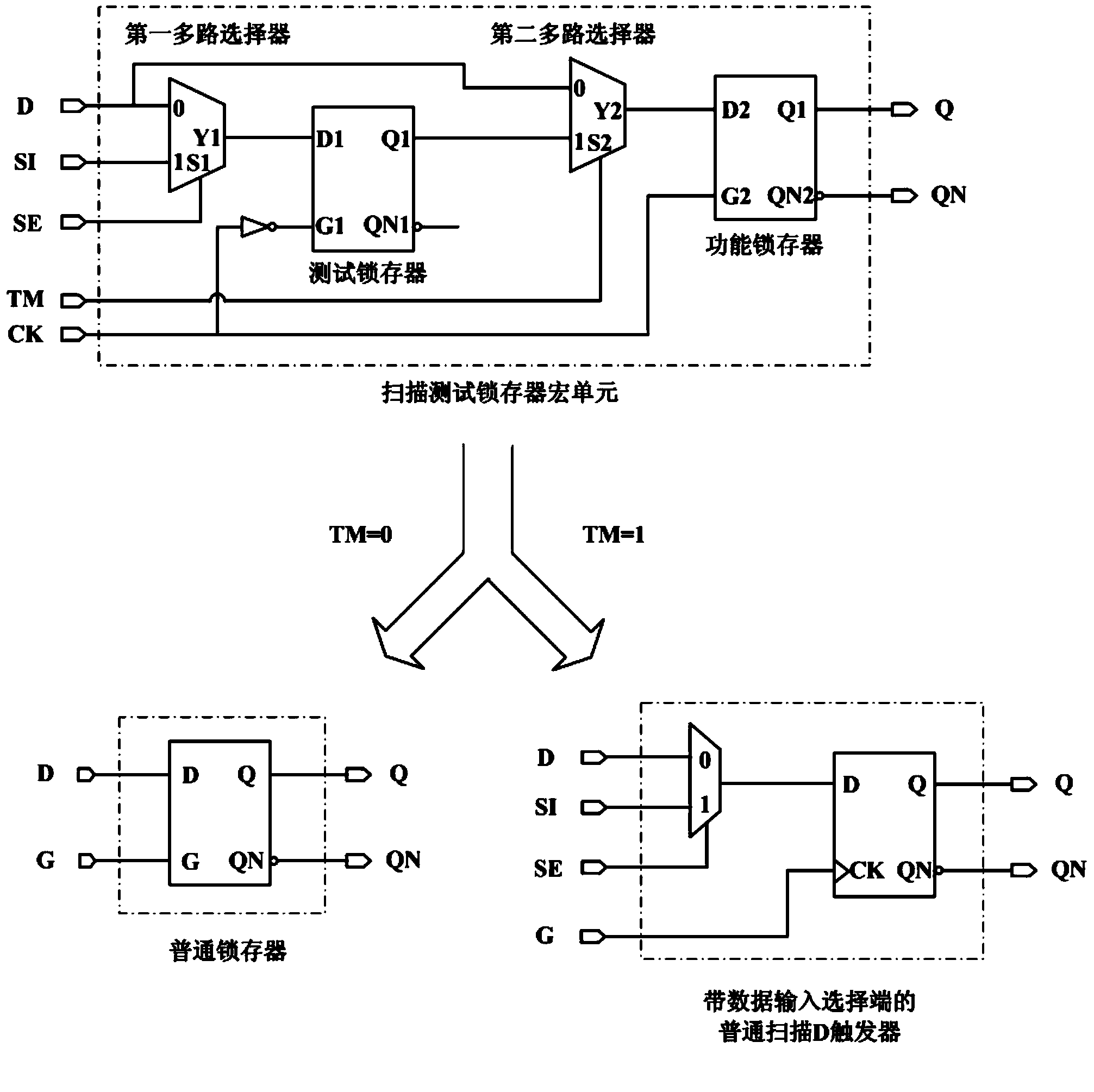
[0037] Such as figure 1 As shown, the realization process of the present invention is first to define the equivalent scan test macrocell model of a common latch unit, it is characterized in that comprising: two latches, an inverter and two multiplexers;

[0038] The two latches are respectively a test latch and a functional latch; the two multiplexers are respectively a first multiplexer and a second multiplexer;

[0039] The 0 data input port (i.e. the first data input port) of the first multiplexer is connected with the data port D, the 1 data input port (i.e. the second data input port) is connected with the scanning input port SI of the macrocell, and the input port is selected S1 is connected to the scan enable port SE of the macrocell, and the data output port Y1 is connected to the input port D1 of the test latch;

[0040] The input port of the inverter is connected to the clock input port CK of the macro unit, and the output port is connected to the latch control sign...


PUM


Abstract

The invention provides a scan test latch macrocell and a scan test method. According to the scan test method, through a customized scan test macrocell, an ATPG test vector, based on a structure, used for a latch unit can be generated with a common scan test design method for a D trigger according to a special design process, the problems that testability design development cannot be easily performed on an existing digital special integrated circuit based on latch design, the fault coverage rate of the test vector is low, and time sequence analysis is complex are solved, the fault coverage rate of chip tests is substantially increased, the effectiveness and the completeness of the chip tests are guaranteed, and the method is mainly applied to the test vector development of the digital special integrated circuit based on latch design.

Description

technical field [0001] The invention relates to a scan test macro unit and a scan test method, in particular to a scan test latch macro unit and a scan test method, which belong to the field of design and test of semiconductor digital integrated circuits, and are mainly used in the structuring of semiconductor digital integrated circuits Testing process. Background technique [0002] With the continuous development and progress of semiconductor digital integrated circuits, how to fully and effectively implement digital integrated circuits with an increasing scale of millions of gates, tens of millions of gates, or even larger scales with reasonable time and cost Testing has gradually become one of the most difficult and time-consuming design tasks. When the circuit scale exceeds 100,000 gates, the development time of hand-written (function-oriented) test vectors will exceed the design time of the actual device itself. Therefore, design for test technology (Design For Test,...

Claims


Application Information

Patent Timeline
Patent Type & Authority Applications(China)
IPC IPC(8): G01R31/317
Inventor 喻贤坤赵元富文治平袁大威姜爽袁超王莉樊旭彭斌
Owner BEIJING MXTRONICS CORP
Why Eureka
Try Eureka