
MOS (metal oxide semiconductor) grid-control thyristor and manufacturing method thereof

A manufacturing method and thyristor technology, which is applied in the direction of thyristor, semiconductor/solid-state device manufacturing, electrical components, etc., can solve the problems of complex manufacturing process and system reliability decline, and achieve the effect of solving complex system and difficult manufacturing process

Active Publication Date: 2015-03-04
UNIV OF ELECTRONICS SCI & TECH OF CHINA
View PDF4 Cites 12 Cited by
  • Summary
  • Abstract
  • Description
  • Claims
  • Application Information

AI Technical Summary

Problems solved by technology

[0004] The purpose of the present invention is to propose a MOS gate-controlled thyristor and its manufacturing method in view of the problem of system reliability decline caused by the complexity of the conventional MGT manufacturing process and the characteristics of normally-on devices.

Method used


Image

  • MOS (metal oxide semiconductor) grid-control thyristor and manufacturing method thereof
  • MOS (metal oxide semiconductor) grid-control thyristor and manufacturing method thereof
  • MOS (metal oxide semiconductor) grid-control thyristor and manufacturing method thereof

Examples


Embodiment Construction

[0045] The present invention is described in detail below in conjunction with accompanying drawing

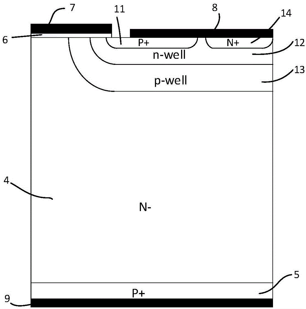
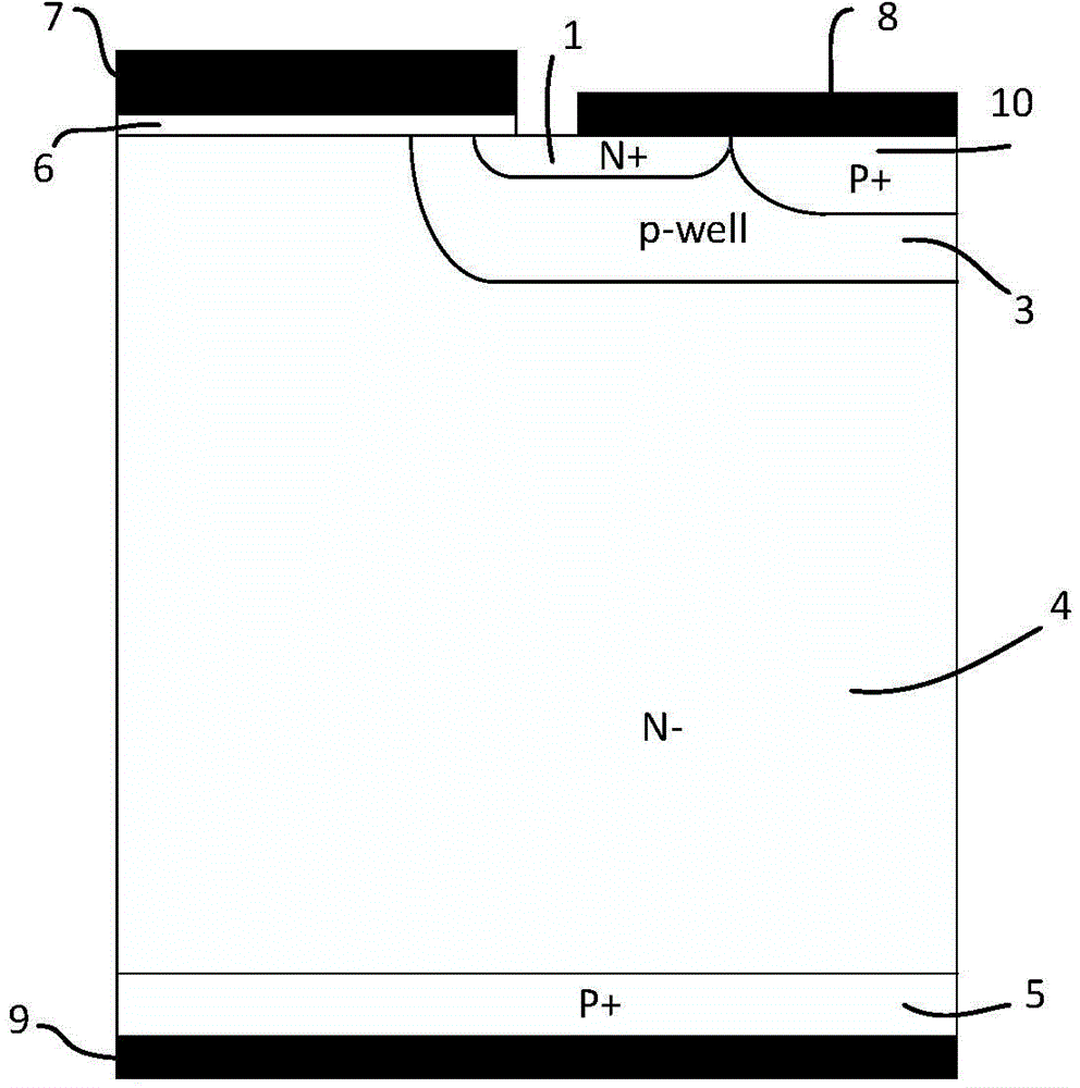
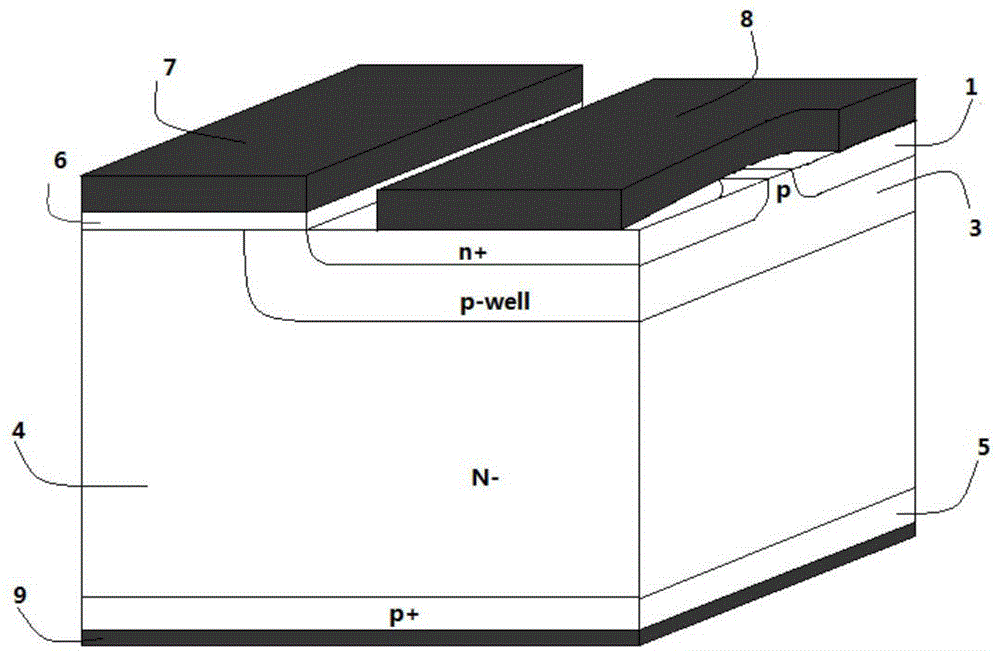
[0046] The MOS gate-controlled thyristor provided by the present invention is characterized in that the gate structure and anode structure are similar to the various gate and anode structures of the existing IGBT, and the planar gate structure cells are such as image 3 and Figure 5 As shown, the trench gate structure cell such as Figure 4 and Figure 6 As shown; the P-type base region 3 has a raised structure passing through the N-type semiconductor source region 1 and partially contacts the cathode metal 8 to form a cathode short circuit structure. Conventional IGBT, such as figure 2 As shown, the P-type base region 3 is fully in contact with the cathode metal 8 through the P+ region 10, and directly extracts holes in the drift region when the IGBT is turned on to suppress the turn-on of the parasitic thyristor and ensure that the IGBT works in a transistor mode. The l...


PUM


Abstract

The invention relates to semiconductor technology, in particular to an MOS (metal oxide semiconductor) grid-control thyristor and a manufacturing method thereof. A cathode of a device is improved into a P-N junction two-layer structure comprising a P-type semiconductor base region and an N-type semiconductor source region. Compared with a conventional MGT (metal gate transistor) cathode P-N-P three-layer structure, the cathode P-N junction two-layer structure uses a double-diffusion process and is simple to manufacture and compatible with an IGBT (insulated gate bipolar transistor) manufacturing process. A device grid lower channel is an N-type channel with normally closed characteristics, extra negative voltage is not needed when the channel is closed, system complexity is reduced, and system reliability is enhanced. The invention is particularly applicable to the MOS grid-control thyristor and manufacture thereof.

Description

technical field [0001] The invention relates to semiconductor technology, in particular to a MOS gate-controlled thyristor and a manufacturing method thereof. Background technique [0002] Power semiconductor devices, as switching devices, can be used in the fields of power electronics and power pulses. MOS gate-controlled thyristors (MOS-Gate Thyristors, MGTs for short) are an emerging family of power semiconductor devices, which have the advantages of low turn-on voltage drop of thyristors, large voltage capacity, high input impedance of MOS devices, and convenient shutdown. Excellent properties such as high current density, low on-state loss and high switching speed are very suitable for applications in the field of power pulses. Since the advent of MGT, its related products have been widely used in the field of power pulse. However, MGT devices also have some disadvantages. Taking the typical MGT structure, MOS-Control Thyristor (MCT for short) as an example: MCT is a ...

Claims


Application Information

Patent Timeline
Patent Type & Authority Applications(China)
IPC IPC(8): H01L29/74H01L29/423H01L21/332
CPCH01L29/41716H01L29/66363H01L29/7455
Inventor 陈万军刘超古云飞程武李震洋肖琨杨骋张波
Owner UNIV OF ELECTRONICS SCI & TECH OF CHINA
Learn More