

Preparation method of polycrystalline black silicon of micro-nano composite suede structure
A micro-nano composite, polycrystalline silicon wafer technology, applied in chemical instruments and methods, crystal growth, final product manufacturing, etc., can solve the problems of fast reaction speed, single, difficult to control reaction process, etc., to reduce the surface reflectivity, reduce the surface Compounding, removal-friendly effect
- Summary
- Abstract
- Description
- Claims
- Application Information
AI Technical Summary
Problems solved by technology
Method used
Image

Examples
Embodiment 1
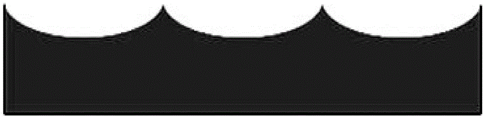
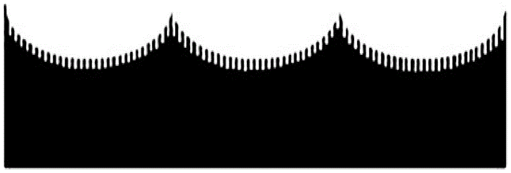
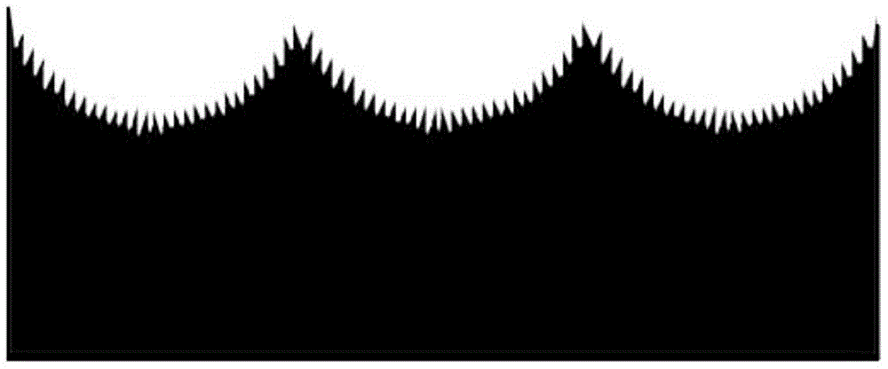
[0031] First, the p-type polysilicon wafer was etched in an etching solution composed of hydrofluoric acid and nitric acid. The concentration of hydrofluoric acid was 2.5 mol / L, and the concentration of nitric acid was 7.5 mol / L. After 100 seconds, it was taken out and Cleaning is carried out to prepare a polycrystalline silicon wafer with a micro-textured structure; then, it is placed in a mixed solution of hydrofluoric acid and silver nitrate, wherein the concentration of hydrofluoric acid is 4 mol / L, and the concentration of silver nitrate is 0.005 mol / L, take it out after standing for 60s, and obtain a polysilicon wafer with silver nanoparticles adsorbed on the micron suede surface; then, put it into the etching solution of hydrofluoric acid and hydrogen peroxide, wherein the concentration of hydrofluoric acid was 4 mol / L, the concentration of hydrogen peroxide was 0.4 mol / L, and the etching time was 1 min, then the polycrystalline silicon wafer with micro-nano composite s...
Embodiment 2
[0033] First, the p-type polysilicon wafer is etched in an etching solution composed of hydrofluoric acid and nitric acid. The concentration of hydrofluoric acid is 2.5 mol / L, and the concentration of nitric acid is 7.5%. After 100s, it is taken out and cleaned. , to prepare a polycrystalline silicon wafer with a micron textured structure; then, place it in a mixed solution of hydrofluoric acid and copper nitrate, wherein the concentration of hydrofluoric acid is 4 mol / L, and the concentration of copper nitrate is 0.005 mol / L , take it out after standing for 60s, and obtain a polysilicon wafer with copper nanoparticles adsorbed on the micron suede surface; then, put it into an etching solution of hydrofluoric acid and hydrogen peroxide, wherein the concentration of hydrofluoric acid is 4 mol / L, the concentration of hydrogen peroxide is 0.4 mol / L, and the etching time is 1 min, then take it out to obtain a polycrystalline silicon wafer with a micro-nano composite texture structu...
Embodiment 3
[0035] First, the p-type polysilicon wafer was etched in an etching solution composed of hydrofluoric acid and nitric acid. The concentration of hydrofluoric acid was 2.5 mol / L, and the concentration of nitric acid was 7.5 mol / L. After 100 seconds, it was taken out and Cleaning is carried out to prepare a polycrystalline silicon wafer with a micro-textured structure; then, it is placed in a mixed solution of hydrofluoric acid and silver nitrate, wherein the concentration of hydrofluoric acid is 4 mol / L, and the concentration of silver nitrate is 0.005 mol / L, take it out after standing for 60s, and obtain a polysilicon chip with silver nanoparticles adsorbed on the micron suede surface; then, put it into the etching solution of hydrofluoric acid and hydrogen peroxide, wherein the concentration of hydrofluoric acid was 4 mol / L, the concentration of hydrogen peroxide was 0.4 mol / L, and the etching time was 1 min, then the polycrystalline silicon wafer with micro-nano composite te...
PUM
 Abstract
Description
Claims
Application Information