A method for preparing fullerene nanostructures

A nanostructure and fullerene technology, applied in the direction of nanotechnology, nanotechnology, nanotechnology for materials and surface science, etc., can solve the problems of difficult realization, complicated process, high cost, etc., and achieve the effect of good structural state

Inactive Publication Date: 2016-04-20
SOUTHEAST UNIV
View PDF0 Cites 0 Cited by
  • Summary
  • Abstract
  • Description
  • Claims
  • Application Information

AI Technical Summary

Problems solved by technology

Although the traditional photolithography process can use the etching method to remove excess fullerenes, the cost is high, the process is complicated, and it may be subject to greater pollution
For the formation of a single fullerene-substrate contact, the traditional process method is also very difficult to achieve
[0005] Therefore, in future single-molecule circuits, when it is necessary to construct such a single fullerene-substrate contact, traditional methods may encounter great difficulties.

Method used


Image

  • A method for preparing fullerene nanostructures
  • A method for preparing fullerene nanostructures
  • A method for preparing fullerene nanostructures

Examples


Embodiment 1

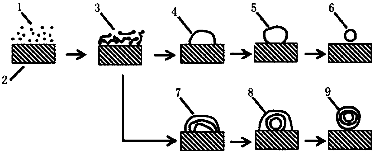
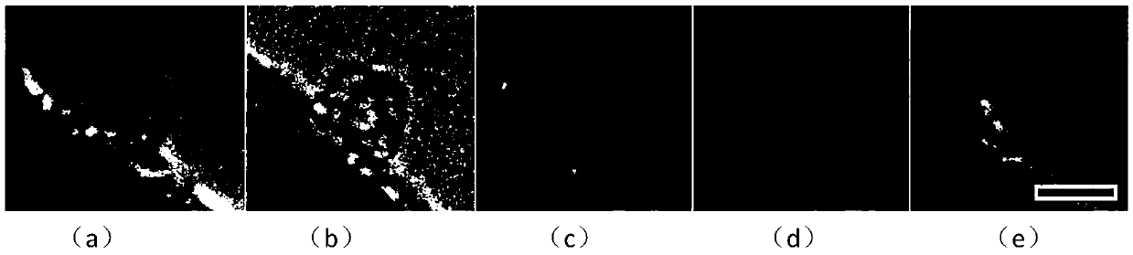
[0023] Implementation example 1: at room temperature, the substrate is made of zinc oxide. The thickness of the amorphous carbon film is about 2 nm. The sample is placed in a vacuum chamber with a vacuum degree of about 1.0×10^(-4)Pa, and the electron beam is turned on to irradiate the designated position. The electron beam intensity is about 1*10 3 e*s^(-1)*nm^(-2). Use a transmission electron microscope to observe the surface condition of the sample at intervals of 2-10 minutes. The result obtained is shown in the figure figure 2 shown. After about 50 minutes of electron beam irradiation, it can be seen that a single monolayer fullerene structure is finally formed at the designated position on the ZnO surface.

Embodiment 2

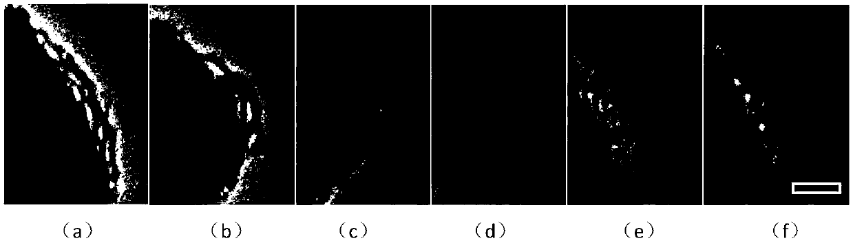
[0024] Implementation example 2: at room temperature, the substrate is made of zinc oxide. The thickness of the amorphous carbon film is about 3.5 nm. The sample is placed in a vacuum chamber with a vacuum degree of about 5.0×10^(-5)Pa, and the electron beam is turned on to irradiate the designated position. Electron beam intensity 1*10 5 e*s^(-1)*nm^(-2). Use a transmission electron microscope to observe the surface condition of the sample at intervals of 2-10 minutes. The result obtained is shown in the figure image 3 shown. After about 70 minutes of electron beam irradiation, it can be seen that a single double-layer fullerene structure is finally formed at the designated position on the ZnO surface.

Embodiment 3

[0025] Implementation example 3: at room temperature, the substrate is made of zinc oxide. The thickness of the amorphous carbon film is about 6 nm. The sample is placed in a vacuum chamber with a vacuum degree of about 1.0×10^(-5)Pa, and the electron beam is turned on to irradiate the designated position. Electron beam intensity 1*10 5 e*s^(-1)*nm^(-2). Use a transmission electron microscope to observe the surface condition of the sample at intervals of 2-10 minutes. The result obtained is shown in the figure Figure 4 shown. After about 100 minutes of electron beam irradiation, it can be seen that a single three-layer fullerene structure is finally formed at the designated position on the ZnO surface.


PUM

PropertyMeasurementUnit
thicknessaaaaaaaaaa
thicknessaaaaaaaaaa
thicknessaaaaaaaaaa

Abstract

The invention provides a preparation method of a fullerene nano structure. The method comprises the following steps: preparing a non-crystal carbon layer with a thickness of 2 to 6 nanometers on the surface of a clean substrate material; then placing the substrate with the non-crystal carbon layer into a vacuum chamber with a vacuum degree of 2*10<-3> or less; starting an electronic gun, and converging the electronic beams to the substrate surface, wherein the bean intensity of the electronic beams is 103-105 e*s^(-1)*nm^(-2); and after 10 to 200 minutes of electronic beam radiation, the fullerene materials are formed on the positions radiated by the electronic beams. Single fullerene particles can be prepared in specific positions individually, fullerene materials with different layers can be obtained, and the structural state of the obtained fullerene material is good.

Description

technical field [0001] The invention relates to a method for high-precision preparation of fullerene nanostructures at specific positions on the surface of materials, in particular to a method for forming fullerene nanostructures on the surface of materials by electron beam irradiation processing, which belongs to the technology of advanced semiconductor material preparation field. Background technique [0002] Fullerene is a special allotrope of carbon. Its special spherical shape makes it have high structural stability. It can be used in the construction of semiconductor devices, advanced functional material additives, solar cells and other fields. Fullerene in a narrow sense refers to C60 molecule, which is composed of 60 carbon atoms to form a perfect spherical shape, so it is also called footballene. Fullerenes in a broad sense include various spherical structures composed of carbon atomic layers, each of which has a graphene-like structure. [0003] At present, there...

Claims


Application Information

Patent Timeline
Patent Type & Authority Patents(China)
IPC IPC(8): C01B31/02B82Y30/00
Inventor 万能万树
Owner SOUTHEAST UNIV
Why Eureka
Try Eureka