Low-thickness and low-cost chip size package with cavity

A chip-size packaging, low-thickness technology, applied in the direction of electric solid devices, semiconductor devices, microstructure devices, etc., can solve the problems of easy generation of fragments, splinters, accelerated device failure, high cost, etc., to reduce peeling stress, improve Reliability and yield improvement effect

A chip-size packaging, low-thickness technology, applied in the direction of electric solid devices, semiconductor devices, microstructure devices, etc., can solve the problems of easy generation of fragments, splinters, accelerated device failure, high cost, etc., to reduce peeling stress, improve Reliability and yield improvement effect

CN104409422AInactive Publication Date: 2015-03-11BEIJING UNIV OF TECH

Image

  • Low-thickness and low-cost chip size package with cavity
  • Low-thickness and low-cost chip size package with cavity
  • Low-thickness and low-cost chip size package with cavity

Examples


Embodiment Construction

[0038] The present invention will be described in more detail below with reference to accompanying drawing:

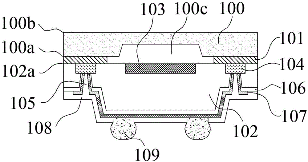
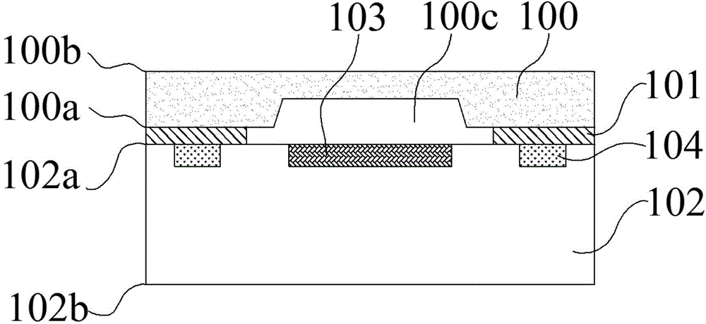
[0039] by figure 1 As shown, a cavity-containing low-thickness low-cost chip size package according to an embodiment of the present invention has a structure comprising:

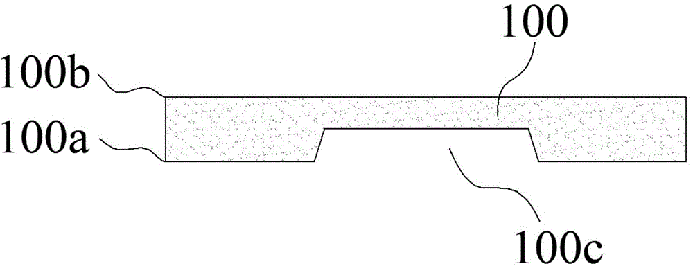
[0040] 1. Cover plate 100, a cavity structure 100c is made on the cover plate front side 100a; 2. Wafer 102, which includes a wafer front side 102a and a wafer back side 102b; 3. Functional area 103 and pad 104, the functional area 103 and pads 104 are distributed on the front surface 102a of the wafer, wherein the pads 104 are distributed around the periphery of the function 103 and realize conduction; 4. The bonding glue 101 is located between the cover plate 100 and the wafer 102, and the 5. TSV 105, the TSV 105 exposes the pad 104, so that the conduction between the pad 104 and the subsequent redistribution layer is realized; 6. The redistribution circuit layer, the The redistribution circuit l...


PUM


Abstract

The invention discloses a low-thickness and low-cost chip size package with a cavity, and belongs to the field of packaging of semiconductors. The package structure comprises a cover plate, a wafer, a function region, bonding pads, bonding glue, silicon through holes, a redistribution circuit layer and a solder ball, wherein a cavity structure is formed in the front surface of the cover plate; the wafer comprises a wafer front surface and a wafer back surface; the function region and the bonding pads are distributed on the wafer front surface; the bonding pads are distributed on the periphery of the function region and are communicated with one another; the bonding glue is positioned between the cover plate and the wafer; the cover plate and the wafer are bonded together by the bonding glue; the bonding pads are exposed via the silicon through holes, so that the bonding pads are communicated with the a follow-up redistribution layer; the redistribution circuit layer is positioned on the wafer back surface and comprises a passivation layer, a metal layer and a solder layer; the bonding pads are communicated with the solder ball via the redistribution circuit layer; and the solder ball is positioned on the redistribution circuit layer of the wafer back surface. The thickness of the package is reduced, and the stress in the structure is also reduced. Moreover, the yield of a cutting process and the reliability of the package are improved.

Description

technical field [0001] The invention relates to a low-thickness and low-cost chip size package with a cavity, which belongs to the field of semiconductor packages. It can be preferably used in image sensors, MEMS devices or integrated chips, etc. Background technique [0002] Chip Scale Package (CSP) is a new generation of chip packaging technology, and its technical performance has been improved again. CSP packaging can make the ratio of chip area to package area exceed 1:1.14, which is quite close to the ideal situation of 1:1. The absolute size is only 32 square millimeters, which is about 1 / 3 of ordinary BGA, which is only equivalent to thin and small One-sixth the area of ​​a TSOP memory chip. Compared with ordinary ball grid array package (BGA), CSP package can increase the storage capacity by three times in the same space. The purpose of CSP is to use high-density chips (chips with more functions, better performance, and more complex chips) to replace previous chip...

Claims


Application Information

Patent Timeline
11 Mar 2015
Publication
CN104409422A
IPC
H01L23/043; H01L23/31; H01L21/50; H01L21/768; H01L27/146; B81B7/02; B81C3/00
CPC
H01L2224/13
Inventors
秦飞; 武伟