High-voltage fast turn-on thyristor and manufacturing method thereof

A thyristor, high-voltage technology, applied in the field of power semiconductor devices, can solve the problems of inability to maintain the technical level and the practicability of di/dt fast turn-on devices, so as to reduce device voltage drop, meet energy saving and consumption reduction, and improve uniformity. Effect

Active Publication Date: 2017-10-27
HUBEI TECH SEMICON
View PDF8 Cites 0 Cited by
  • Summary
  • Abstract
  • Description
  • Claims
  • Application Information

AI Technical Summary

Problems solved by technology

[0004] According to this conventional process and characteristic requirements, the on-state voltage drop of the fast device has reached about 3.2V, which is unable to maintain the original technical level and improve the withstand voltage to above 4500V; the di / dt of the pulse device of the original process has reached 1500 A / µs limit value
The traditional technology no longer has the practicability of 4500V and higher di / dt fast turn-on devices

Method used


Image

  • High-voltage fast turn-on thyristor and manufacturing method thereof
  • High-voltage fast turn-on thyristor and manufacturing method thereof
  • High-voltage fast turn-on thyristor and manufacturing method thereof

Examples


Embodiment 1

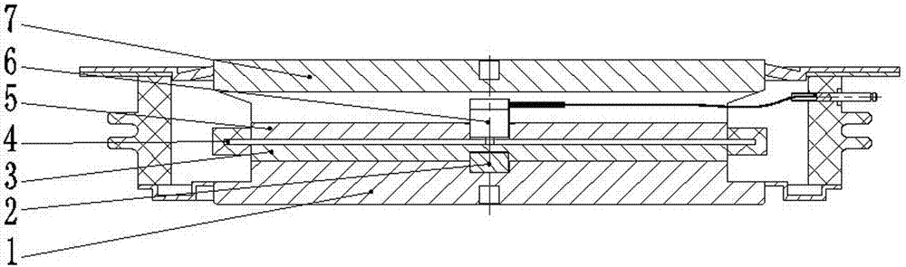
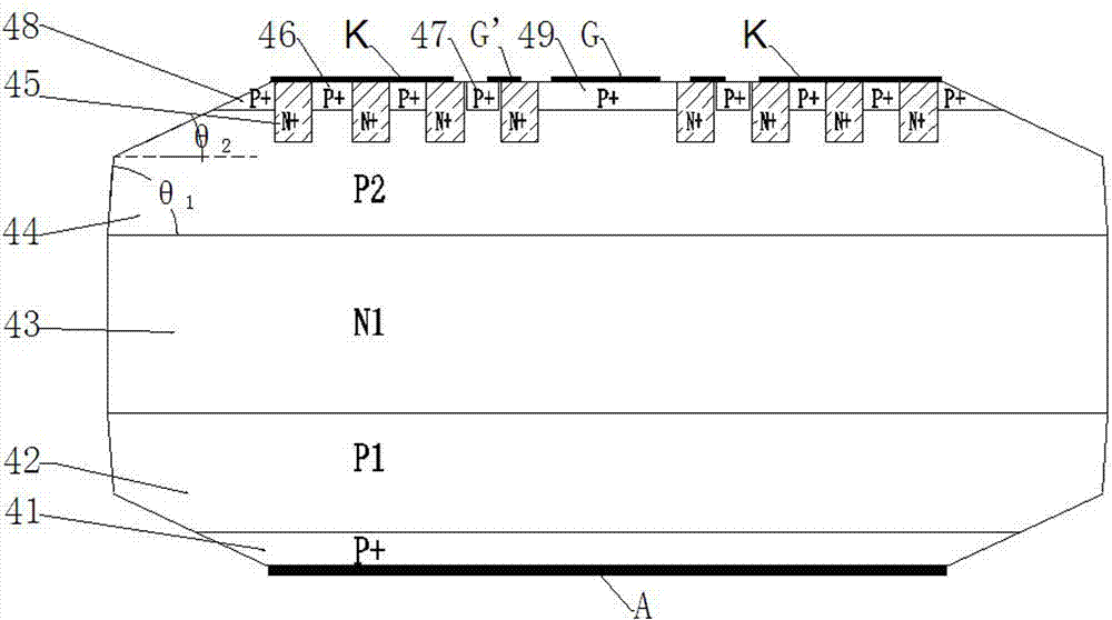
[0046] Example 1 as figure 1 , figure 2 , Figure 9 As shown, it is a high-voltage fast turn-on thyristor designed according to 5000V, and the chip size is 101.6mm. It is packaged by the lower sealing part 1 of the tube case, the lower gasket 3 , the semiconductor chip 4 , the upper gasket 5 , the gate assembly 6 and the upper sealing part 7 . A positioning column 2 is provided between the lower gasket 3 and the lower sealing part 1 of the tube case. The semiconductor chip 4 is a three-terminal PNPN four-layer structure, and the three terminals are respectively the anode A, the cathode K and the gate, and the gate includes the center gate G and the amplification gate G', and the PNPN four-layer structure is respectively the P1 anode region 42 , N1 long base region 43 , P2 short base region 44 and N+ cathode region 45 . An anode P+ layer 41 is added on the surface of the anode area of ​​the chip P1, and a cathode P+ layer is provided on the cathode surface of the central g...

Embodiment 2

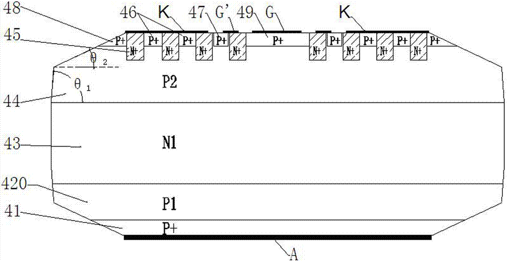
[0053] Example 2 as figure 1 , image 3 , Image 6 , Figure 9 As shown, the difference with embodiment 1 is that the chip adopts such as Image 6 process, the junction depth of the P1 anode region is 30∽110 μm, and the P1 anode region 420 is 30∽50 μm shallower than the P2 short base region 44 . This design reduces the thickness of the silicon wafer, which further reduces the voltage drop of the device. This product is suitable for fast turn-on devices with low reverse blocking voltage or no reverse blocking voltage.

Embodiment 3

[0054] Example 3 as Figure 4 As shown, the difference from Embodiment 1 and Embodiment 2 is that the mesa of the semiconductor chip is in the shape of a double positive angle mesa. The size of the positive angle θ11 is: 20º≤θ11≤80º. The product of this embodiment has the smallest cathode area loss, and is suitable for fast turn-on devices with the same diameter and larger current.


PUM


Abstract

The invention relates to a high-voltage quick-turn-on thyristor and a manufacturing method thereof, and belongs to the technical field of power semiconductor devices. The thyristor mainly solves the disadvantages that a cathode of the existing semiconductor device has low di / dt tolerance, poor gate-controlled turn-on uniformity and the like due to the fact that an involute unit of an amplifier gate is too long. The thyristor is mainly characterized in that a semiconductor chip is in a three-terminal PNPN four-layer structure; three terminals are an anode, a cathode and a gate; the PNPN four-layer structure is divided into a P1 anode region, an N1 long base region, a P2 short base region and N+ cathode regions; an anode P+ layer is additionally arranged on the surface of the P1 anode region; and central gate, amplifier gate, short-circuit point and short-circuit ring regions on the surface of the cathode region are provided with P+ layers. The thyristor has the characteristics of reducing the transverse resistance at the gate and a short-circuit point, reducing the voltage drop of a device, improving the uniformity of gate-triggerred turn-on and the turn-on speed of a high-voltage device, and satisfying energy conservation and consumption reduction, and is mainly applied to equipment such as a high-power pulse power supply and a high-power serial inversion power supply.

Description

technical field [0001] The invention belongs to the technical field of power semiconductor devices. It specifically relates to a semiconductor switch device with a high voltage above 4000V, which is mainly used in high-power pulse power supply and series inverter power supply devices. Background technique [0002] The conventional fast turn-on thyristor is a PNPN four-layer three-terminal structure device. The usual manufacturing method is to directly perform P-type diffusion on both ends of the N-type silicon to form a symmetrical PNP structure, and then perform N-type selective diffusion in the P region of the cathode end. Finally, a PNPN structure is formed, and the doping depth and impurity concentration distribution of the anode region of P1 and the cathode region of P2 are the same. The conventional blocking voltage of the fast turn-on thyristor device of this structure is 1200V∽2500V. Using stepwise diffusion in P1 and P2 areas, and adding a P+ layer structure device...

Claims


Application Information

Patent Timeline
Patent Type & Authority Patents(China)
IPC IPC(8): H01L29/74H01L29/06H01L21/332H01L29/43
CPCH01L29/0834H01L29/0839H01L29/1012H01L29/66363H01L29/74
Inventor 张桥刘鹏颜家圣邢雁吴拥军杨宁肖彦刘小俐任丽
Owner HUBEI TECH SEMICON
Why Eureka
Try Eureka