Light-emitting diode element, and method for manufacturing light-emitting diode element

A technology of light-emitting diodes and manufacturing methods, which is applied in the direction of electrical components, semiconductor devices, circuits, etc., can solve the problems of high price, inability to realize the physical potential of nitride semiconductors, large crystal orientation deviation of dislocation density substrates, etc., and reduce lateral resistance Effect

Active Publication Date: 2022-04-15
PANASONIC INTELLECTUAL PROPERTY MANAGEMENT CO LTD
View PDF23 Cites 0 Cited by
  • Summary
  • Abstract
  • Description
  • Claims
  • Application Information

AI Technical Summary

Problems solved by technology

[0003] Conventionally, heterogeneous substrates such as sapphire and Si have been used as substrates for forming III-nitride semiconductor devices, and III-nitride semiconductor thin films formed on these heterogeneous substrates have high dislocation densities, making it impossible to realize the inherent physical potential of nitride semiconductors.
Although a GaN substrate with a lower dislocation density than this heterogeneous substrate has been commercialized, there is still a problem that the dislocation density and the crystal orientation of the substrate are large, and the problem is that it is expensive

Method used


Image

  • Light-emitting diode element, and method for manufacturing light-emitting diode element
  • Light-emitting diode element, and method for manufacturing light-emitting diode element
  • Light-emitting diode element, and method for manufacturing light-emitting diode element

Examples


Deformed example 1

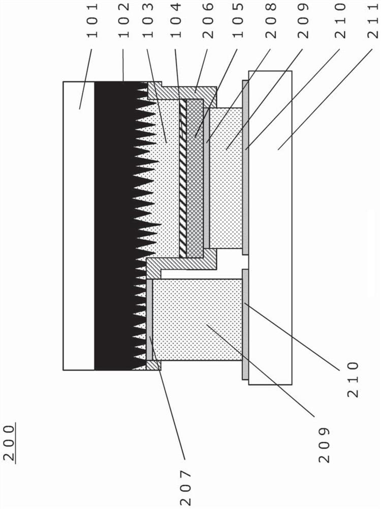
[0114] Figure 8 It is a diagram showing the configuration of a light emitting diode element 200 according to Modification 1. FIG.

[0115] The light emitting diode element 200 of Modification 1 is different from the above-mentioned embodiment in that the surface on which the n-side ohmic electrode 207 is formed is a surface where only the second n-type GaN layer 103 is exposed.

[0116] Figure 8 In this process, the etching by dry etching in the above etching step (step S12 ) is reduced so that the surface on which the n-side ohmic electrode 207 is formed is in the second n-type GaN layer 103 . For example, such a configuration may be adopted when it is desired to reduce the etching level difference by dry etching.

[0117] In the light emitting diode element 200 of this modified example, there is a possibility that the resistance may be reduced by increasing the thickness of the n-type semiconductor layer. However, on the other hand, the contact resistance of the n-side ...

Deformed example 2

[0119] Figure 9 It is a figure showing the structure of the light emitting diode element 200 of the modification 2.

[0120] The light emitting diode element 200 of Modification 2 is different from the above-mentioned embodiment in that the surface on which the n-side ohmic electrode 207 is formed is a surface where only the first n-type GaN layer 102 is exposed.

[0121] Figure 9 In this case, the surface on which the n-side ohmic electrode 207 is formed is in the first n-type GaN layer 102 . For example, when the thickness of the first n-type GaN layer 102 is sufficiently thick, or when the unevenness is small and it is difficult to stop etching at the interface, such a structure can simplify the process steps.

[0122] In the light emitting diode element 200 of this modified example, the contact resistance of the n-side ohmic electrode 207 can be reduced the most. On the other hand, however, the substrate resistance caused by the first n-type GaN layer 102 directly und...

Deformed example 3

[0124] In the above-mentioned embodiments, a scheme in which the second n-type GaN layer 103 is formed through a single crystal growth process is shown. However, when the unevenness of the first n-type GaN layer 102 is very large, it is difficult to make the surface of the second n-type GaN layer 103 completely flat, and there is a concern that some Concavity and convexity of about 100 nm. In addition, there is a concern that the thickness of the second n-type GaN layer 103 becomes too thick for planarization.

[0125] Therefore, in the process of forming the second n-type GaN layer 103 , mechanical polishing and CMP (Chemical Mechanical Polishing) may be performed on the second n-type GaN layer 103 . For example, after the second n-type GaN layer 103 is crystal-grown by the HVPE method, mechanical polishing may be performed, and the second n-type GaN layer 103 may be crystal-grown again by the MOCVD method or the like.

[0126] With such a configuration, unevenness formed o...


PUM

PropertyMeasurementUnit
thicknessaaaaaaaaaa
thicknessaaaaaaaaaa
thicknessaaaaaaaaaa

Abstract

The present invention provides a flip chip type light emitting diode element capable of reducing lateral resistance. The flip-chip type light-emitting diode element has a carrier concentration of 1×10 stacked sequentially. 19 cm ‑3 More than and less than 3×10 20 cm ‑3 The first n-type group III nitride semiconductor layer (102), the carrier concentration is 5×10 17 cm ‑3 More than and less than 1×10 19 cm ‑3 A laminate structure of a second n-type III-nitride semiconductor layer (103), a light-emitting layer (104) made of a III-nitride semiconductor, and a p-type III-nitride semiconductor layer (105), the first The height difference between the n-type III-nitride semiconductor layer (102) and the second n-type III-nitride semiconductor layer (103) is greater than that of the second n-type III-nitride semiconductor layer (103) The height difference of the concavity and convexity of the interface with the light-emitting layer (104).

Description

technical field [0001] The invention relates to a light emitting diode element and a method for manufacturing the light emitting diode element. Background technique [0002] Group III nitride-based compound semiconductors represented by gallium nitride (GaN), so-called nitride semiconductors, have attracted much attention as materials for new devices such as light-emitting diodes (LEDs), laser diodes (LDs), and power devices. The nitride semiconductor is a general formula composed of In x Ga y al 1-x-y N (0≤x≤1, 0≤y≤1, x+y≤1), containing indium (In), gallium (Ga), and aluminum (A1) as group III elements, and as group V elements Nitrogen (N) compound semiconductor. [0003] Conventionally, heterogeneous substrates such as sapphire and Si have been used as substrates for forming III-nitride semiconductor devices, and III-nitride semiconductor thin films formed on these heterogeneous substrates have high dislocation densities, making it impossible to realize the inherent ph...

Claims


Application Information

Patent Timeline
Patent Type & Authority Patents(China)
IPC IPC(8): H01L33/24H01L33/32H01L33/00
CPCH01L33/325H01L33/007H01L33/24H01L33/22H01L33/32H01L33/025H01L33/14H01L33/0075
Inventor 大野启山下贤哉
Owner PANASONIC INTELLECTUAL PROPERTY MANAGEMENT CO LTD
Why Eureka
Try Eureka