Schottky diode die and preparation method thereof, diode and photovoltaic module

A Schottky diode and Schottky potential technology, applied in the manufacturing of electrical components, semiconductor devices, semiconductor/solid-state devices, etc., can solve the problem of increased die and device thickness, poor conductivity of backfill polysilicon, and increased device series resistance, etc. question

Inactive Publication Date: 2019-11-22
SUZHOU CHENGBANG DALI MATERIAL TECH
View PDF0 Cites 0 Cited by
  • Summary
  • Abstract
  • Description
  • Claims
  • Application Information

AI Technical Summary

Problems solved by technology

[0012] (1) The grooves in the trenched Schottky diodes create stress in the silicon, making the die prone to cracking
In order to overcome this shortcoming, the existing technology will backfill the trench with polysilicon after doping in the trench, which increases the process cost;
[0013] (2) Since the electrical conductivity of the backfilled polysilicon is worse than that of metal, the ability of the prior art to increase the surge current of the Schottky diode will be adversely affected;
[0014] (3) The arrangement of grooves increases the local current density, and the flow of substrate lateral current must bypass the "isolation wall" formed by the grooves, thus increasing the series resistance of the device;
[0016] (5) Another deficiency of the prior art is that the cathode of the Schottky diode is drawn out from the substrate surface. For the bypass diodes packaged in the photovoltaic module, the thickness of the tube core and the device will increase due to double-sided wiring. , is not conducive to integrated package

Method used


Image

  • Schottky diode die and preparation method thereof, diode and photovoltaic module
  • Schottky diode die and preparation method thereof, diode and photovoltaic module
  • Schottky diode die and preparation method thereof, diode and photovoltaic module

Examples


Embodiment 1

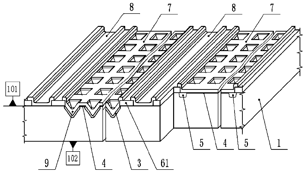
[0090] Please refer to figure 1 , is a schematic structural diagram of a Schottky diode die provided in the present disclosure. The Schottky diode die includes a single crystal silicon substrate 1, a Schottky barrier junction 4, a control PN junction 3, a protection PN junction 5, an isolation medium 61, a die positive electrode contact metal 7 and a die negative electrode In contact with the metal 8, a plurality of etch pits 9 are arranged on the first side 101 of the single crystal silicon substrate 1, and the plurality of etch pits 9 are regularly arranged on the first side 101 of the single crystal silicon substrate 1, and the control PN junction 3 is arranged on On the pit wall of the etching pit 9, the Schottky barrier junction 4 is arranged on the plane adjacent to the control PN junction 3 on the first side 101 of the single crystal silicon substrate 1, and the protection PN junction 5 is arranged on the Schottky barrier junction 4 The edge that is not adjacent to the...

Embodiment 2

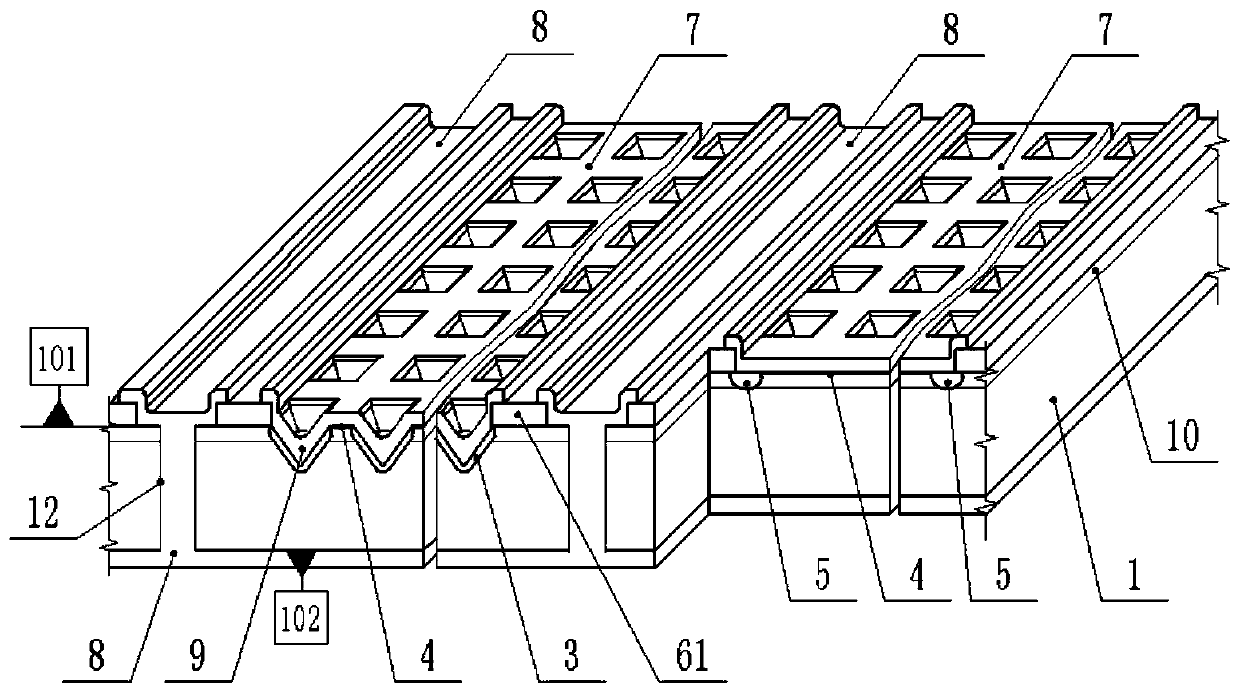
[0111] Please refer to figure 1 , Figure 4 , Figure 5 to Figure 16 , Figure 4 A flow chart of the Schottky diode die manufacturing method provided by the present disclosure, Figure 5 to Figure 16 is a schematic diagram of each process step.

[0112] Step 101, using N-type (100) single crystal silicon substrate 1, such as Figure 5 ;

[0113] In step 102, an isolation dielectric process layer 6 is prepared on the first side 101 and the second side 102 of the single crystal silicon substrate 1 to obtain the following Image 6 The first middleware shown;

[0114] Step 103, on the isolation dielectric process layer 6, prepare the etching pit 9 / control the doping process window 31 of the PN junction 3, and obtain the following Figure 7 The second middleware shown in;

[0115] Step 104, through the etching pit 9 / controlling the doping process window 31 of the PN junction 3, using an alkaline anisotropic etching solution to prepare the etching pit 9 to obtain the followi...

Embodiment 3

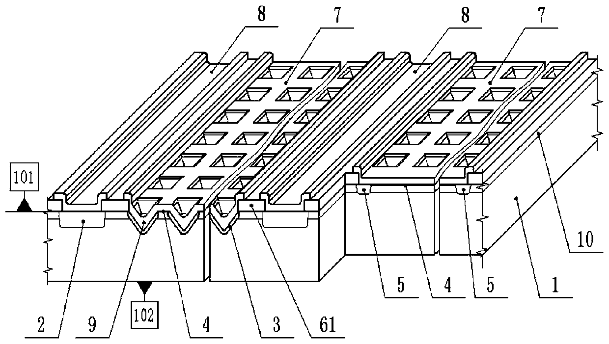
[0125] Please refer to figure 2 , Figure 17 , Figure 18 .

[0126] The difference between this embodiment and embodiment 2 is:

[0127] refer to Figure 17 , using N-type (100) silicon epitaxial wafers as monocrystalline silicon substrate 1, epitaxial layer 10 is N - Silicon, thickness 2μ~20μ;

[0128] In order to realize the ohmic contact between the die negative electrode contact metal 8 and the single crystal silicon substrate 1, before depositing the contact metal 13 in the process window 36 of the die negative electrode contact metal 8, it is necessary to pass through N + Silicon doping prepares heavily doped region 2 of the substrate. The process for preparing the heavily doped region 2 of the substrate is a conventional process in the prior art, so details are not repeated here.

[0129] In this embodiment, the Schottky barrier junction 4 is arranged in the epitaxial layer 10, the substrate heavily doped region 2 penetrates the epitaxial layer 10, and the etch...


PUM


Abstract

The invention provides a Schottky diode core and a preparation method thereof, a diode and a photovoltaic module, and relates to the technical field of photovoltaic power generation. The diode core comprises a monocrystalline silicon substrate, a Schottky barrier junction, control PN junctions, a protection PN junction, an isolation medium, diode core positive electrode contact metal and diode core negative electrode contact metal. The first side surface is provided with a plurality of corrosion pits, the control PN junctions are arranged on the walls of the corrosion pits, and the diode corepositive electrode contact metal and the diode core negative electrode contact metal are led out from the first side surface. According to the invention, high-frequency pulse current and surge currentcan be better reduced, the stress of the diode die is small, and integrated packaging is facilitated.

Description

technical field [0001] The present disclosure relates to the technical field of photovoltaic power generation, in particular, to a Schottky diode tube core, a manufacturing method thereof, a diode and a photovoltaic module. Background technique [0002] Schottky diode is a kind of hot carrier diode based on the principle of metal-semiconductor junction formed by metal-semiconductor contact, also known as metal-semiconductor (contact) diode or surface barrier diode. The application of Schottky diodes in the field of photovoltaic power generation mainly takes advantage of its low forward conduction voltage drop to achieve the purpose of less power loss, so it is widely used in photovoltaic modules as bypass diodes. Due to the particularity of low voltage, high current, and the risk of lightning induction in the installation site of photovoltaic modules, bypass diodes are required to have strong overcurrent capability, anti-surge current capability and certain reverse withstand...

Claims


Application Information

Patent Timeline
Patent Type & Authority Applications(China)
IPC IPC(8): H01L29/872H01L29/06H01L21/329
CPCH01L29/0615H01L29/66143H01L29/872
Inventor 闫勇
Owner SUZHOU CHENGBANG DALI MATERIAL TECH
Why Eureka
Try Eureka