
Method for nondestructively transferring graphene from metal surface to surface of target substrate

A graphene surface and target substrate technology, applied in the field of materials, can solve problems such as resource consumption and graphene damage, and achieve the effects of improving quality, reducing damage, and efficient transfer

Active Publication Date: 2015-03-25
INST OF MICROELECTRONICS CHINESE ACAD OF SCI
View PDF5 Cites 27 Cited by
  • Summary
  • Abstract
  • Description
  • Claims
  • Application Information

AI Technical Summary

Problems solved by technology

The existing transfer methods include direct contact and non-direct contact to clean and transfer graphene. However, these two methods will cause damage to graphene or consume a lot of resources.

Method used


Image

  • Method for nondestructively transferring graphene from metal surface to surface of target substrate
  • Method for nondestructively transferring graphene from metal surface to surface of target substrate
  • Method for nondestructively transferring graphene from metal surface to surface of target substrate

Examples


Embodiment 1

[0044] Embodiment 1: The transfer of CVD graphene on the surface of copper foil to the surface of glass is realized by electrostatic interaction.

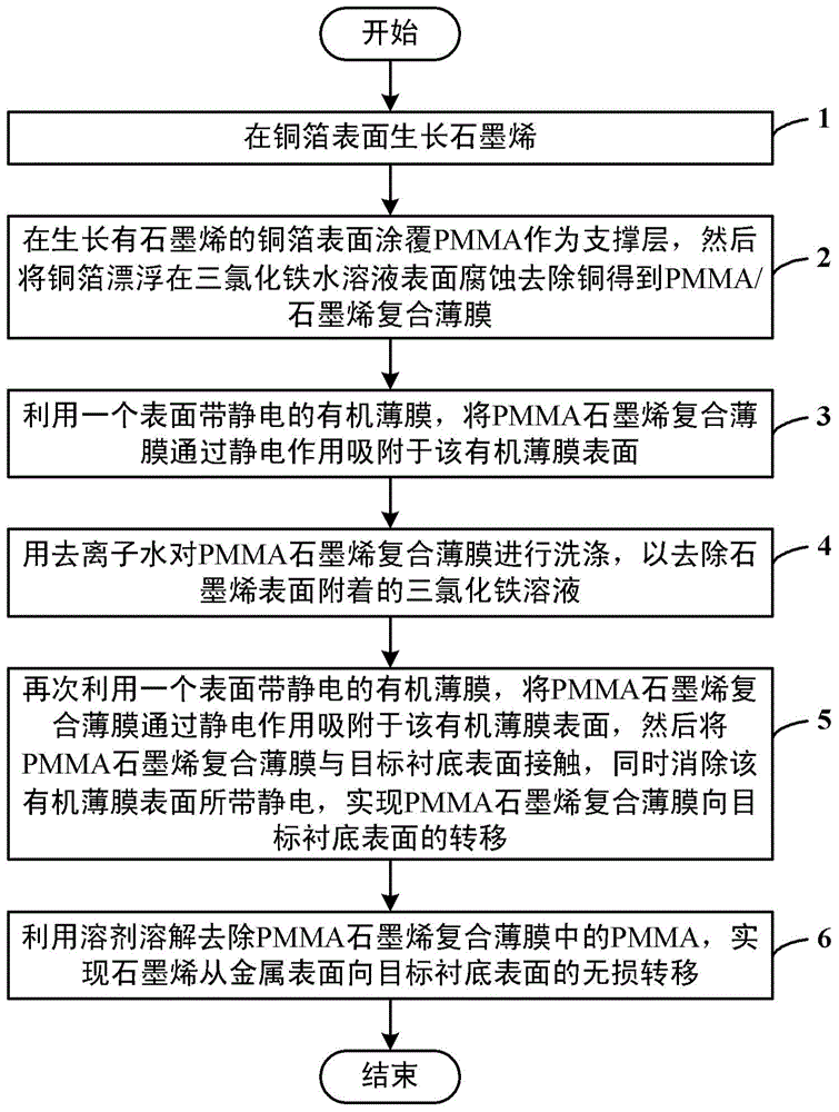
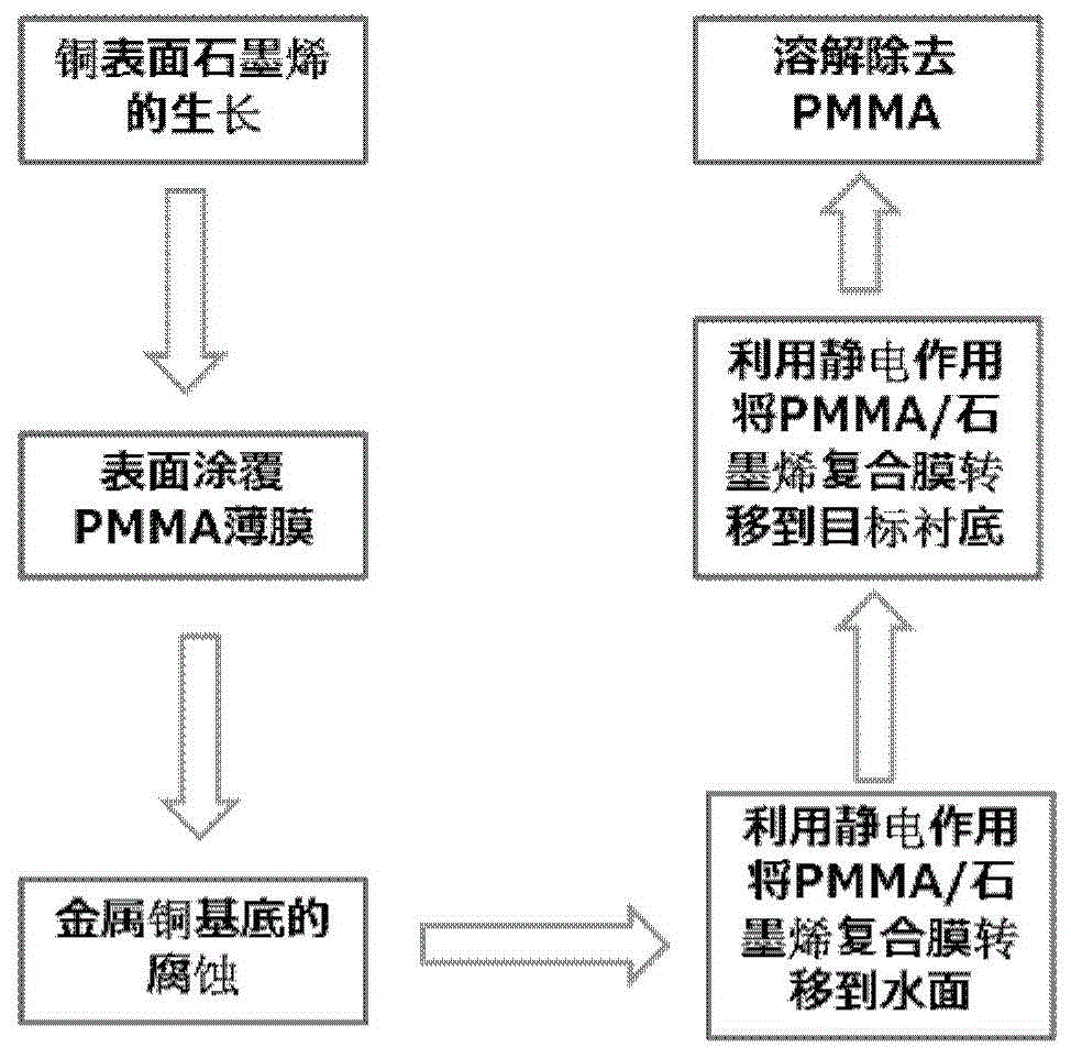
[0045] Put the copper foil into a CVD furnace, in a mixed atmosphere of 10sccm hydrogen and 2sccm methane, use chemical vapor deposition to grow graphene on the copper surface at a high temperature of 1000°C; coat PMMA on the surface of the copper foil with graphene grown; Copper foil floats on the surface of ferric chloride aqueous solution and corrodes to remove metal copper to obtain PMMA / graphene composite film; utilize silk to rub one surface of polyethylene terephthalate (PET) film to make it electrostatically charged, and then PET film The other surface that is not rubbed is close to the PMMA / graphene composite film floating on the ferric chloride solution, and it is adsorbed on the surface of the PET film by electrostatic action; the PMMA / graphene composite film adsorbed on the surface of the PET film is contacted with deion...

Embodiment 2

[0046] Embodiment 2: The transfer of CVD graphene on the surface of copper foil to the surface of PET is realized by electrostatic interaction.

[0047] The specific steps are similar to those in Example 1, but the final target substrate used is PET film.


PUM


Abstract

The invention discloses a method for nondestructively transferring graphene from a metal surface to the surface of a target substrate. The method comprises the steps of enabling graphene to grow on the surface of metal copper; coating the surface of graphene with a PMMA film, floating a copper substrate in an etching agent solution to corrode and remove the copper to obtain a PMMA / graphene composite film; enabling a PET film with static electricity in a friction manner to approach the PMMA / graphene composite film which is floated on the liquid surface, and adsorbing the graphene / PMMA composite film on the surface of the PET film by utilizing the electrostatic effect, contacting the graphene / PMMA composite film with the deionized water, meanwhile, releasing static electricity on the surface of the PET film, separating the PMMA / graphene composite film from the PET film, and floating the PMMA / graphene composite film on the water surface; repeating the steps, washing graphene, and completely removing the copper etching agent attached to the surface of the graphene; and finally transferring the PMMA / graphene composite film to the surface of the target substrate, and dissolving and removing the PMMA on the surface. By utilizing the method, not only can the location transfer of the large-sized graphene be realized, but also the damage rate of the graphene can be greatly reduced.

Description

technical field [0001] The invention belongs to the technical field of materials, in particular to a method for non-destructive transfer of graphene from a metal surface to a target substrate surface. Background technique [0002] In 2004, Professor Geim of the University of Manchester prepared graphene for the first time [K.S.Novoselov, A.K.Geim, S.V.Morozov, D.Jiang, Y.Zhang, S.V.Dubonos, I.V.Grigorieva, A.A.Firsov, Science 2004, 306, 666.]. Graphene is a hexagonal honeycomb-like two-dimensional structure composed of a single layer of carbon atoms. The intrinsic electron mobility of graphene film can reach 200000cm at room temperature 2 / Vs, with excellent electrical properties [K.I.Bolotin, K.J.Sikes, Z.Jiang, M.Klima, G.Fudenberg, J.Hone, P.Kim, H.L.Stormer, Solid State Communications 2008, 146, 351.]. In addition, graphene has extremely high light transmittance in the entire visible light region, and studies have found that the light transmittance of single-layer grap...

Claims


Application Information

Patent Timeline
Patent Type & Authority Applications(China)
IPC IPC(8): C23C16/01C23C16/26C23C16/56
CPCC01B32/186C23C16/01C23C16/26C23C16/56
Inventor 张大勇金智史敬元麻芃王选芸
Owner INST OF MICROELECTRONICS CHINESE ACAD OF SCI
Learn More