OLED display device array substrate and preparation method thereof

A technology for array substrates and display devices, which is applied in the manufacture of semiconductor/solid-state devices, semiconductor devices, and electric solid-state devices, etc., can solve the problems of complex preparation methods of array substrates for OLED display devices, and compensate for spatial inhomogeneity and instability. , the effect of high mobility and few preparation steps

Active Publication Date: 2015-03-25
KUNSHAN GO VISIONOX OPTO ELECTRONICS CO LTD
View PDF5 Cites 7 Cited by
  • Summary
  • Abstract
  • Description
  • Claims
  • Application Information

AI Technical Summary

Problems solved by technology

[0009] For this reason, what the present invention aims to solve is the complicated problem of the preparation method of the array substrate of the OLED display device in the prior art, and provides a method for preparing the array substrate with a simple process, and the array substrate prepared by the method

Method used


Image

  • OLED display device array substrate and preparation method thereof
  • OLED display device array substrate and preparation method thereof
  • OLED display device array substrate and preparation method thereof

Examples


Embodiment 1

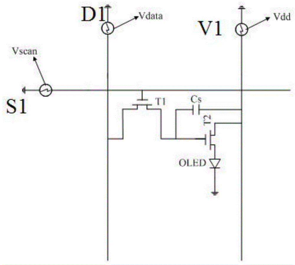
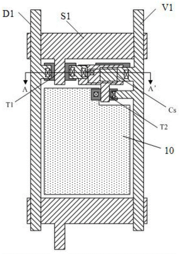
[0049] This embodiment provides a method for preparing an array substrate of an OLED display device and an array substrate prepared by the method. The pixel structure in the basic array is as attached image 3 As shown, the pixel structure includes: a scan line S1 , a data line D1 , a power line V1 , a storage capacitor Cs, a switch TFT T1 , a control TFT T2 and a pixel area 10 .

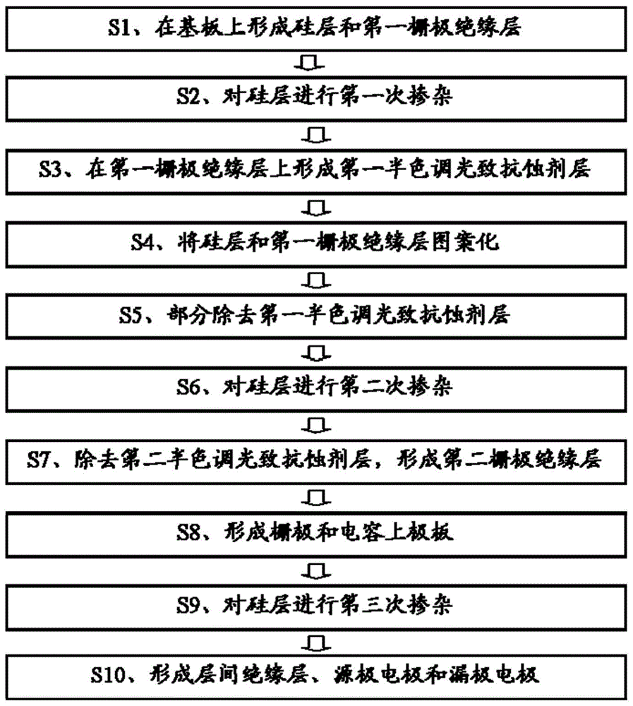
[0050] A flow chart of a method for preparing an OLED display device array substrate provided in this embodiment is shown in the attached figure 2 As shown, the cross-sectional view corresponding to the preparation of the array substrate of the OLED display device is as follows Figure 4 to Figure 12 shown.

[0051] A method for preparing an OLED display device array substrate provided in this embodiment includes the following steps:

[0052] S1, such as Figure 4 As shown, a buffer layer 2 , a semiconductor layer 3 and a first gate insulating layer 41 are sequentially formed on a substrate 1 i...

Embodiment 2

[0070] This embodiment provides a method for preparing an OLED display device array substrate and the array substrate prepared by this method. area 31 width (as Figure 13 shown). When viewed along the thickness direction of the substrate 1, the width L1 of the gate 61 is smaller than the width L2 of the first doped region 31. At this time, the semiconductor layer 3 is doped with P-type ions for the third time. 5×10 14 / cm 2 , to be less than the doping dose of the second doping process 5×10 15 / cm 2 ,, due to the self-alignment of the gate and the relationship that it acts as a mask, the semiconductor layer 3 in the capacitor region will not be doped, and the second doped region 32 in the transistor region is partially heavily doped, forming the third doped region The regions in 34 that have been doped three times at both ends are the source region and the drain region; the region adjacent to the source region and the drain region and that has been doped twice becomes th...


PUM


Abstract

The invention provides an OLED display device array substrate preparation method. Doping of different function regions such as a channel region, a source region, a drain region, an LDD region and a capacitor lower pole plate is realized through two masks and three ion doping steps, the preparation requires fewer steps, and the process is simple. The three doping steps are implemented under the condition of spacing by a gate insulation layer, the same accelerating voltage can be applied, the process cost is saved, and the stability of the process and the yield of devices are improved. The accelerating voltage is the same, and a rapid thermal treatment process is not needed after the completion of the doping process, thus simplifying the process steps. A whole semiconductor layer is doped before the semiconductor layer is patterned, and after a TFT is formed, the carrier mobility of the TFT channel region is increased, a small drift value is given to the threshold voltage (Vth), the space heterogeneity and instability of the TFT are compensated successfully, and the brightness (gray) of pixels can be accurately controlled by controlling the magnitude of current of each pixel unit.

Description

technical field [0001] The invention relates to the field of active-matrix organic light-emitting display devices, in particular to a method for preparing an array substrate of an active-matrix organic electroluminescence display and the array substrate prepared by the method. Background technique [0002] Organic Light-Emitting Diode (English full name Organic Light-Emitting Diode, referred to as OLED) is an active light-emitting device, which has the advantages of high contrast, wide viewing angle, low power consumption, and thinner volume. It is expected to become the next-generation mainstream flat-panel display technology. It is one of the most concerned technologies in display technology. [0003] Active Matrix Organic Light-Emitting Display (English full name Active Matrix organic lighting emitting display, referred to as AMOLED) uses thin film transistors (English full name Thin Film Transistor, referred to as TFT), with capacitor storage signals to control the brigh...

Claims


Application Information

Patent Timeline
Patent Type & Authority Applications(China)
IPC IPC(8): H01L21/77H01L27/32
CPCH01L21/77H01L2021/775H10K59/12
Inventor 向长江邱勇
Owner KUNSHAN GO VISIONOX OPTO ELECTRONICS CO LTD
Why Eureka
Try Eureka