

Texturing preprocessing method of diamond wire cut polycrystalline silicon chip, textured preprocessed silicon chip and application thereof
A diamond wire cutting, polycrystalline silicon wafer technology, applied in the direction of post-processing, post-processing details, chemical instruments and methods, etc., can solve the problems of new cutting process silicon wafers cannot be mass-produced, irregular texture, low battery conversion efficiency, etc. , to achieve the effect of simple texturing pretreatment method, low reflectivity and short processing time
- Summary
- Abstract
- Description
- Claims
- Application Information
AI Technical Summary
Problems solved by technology
Method used
Image

Examples
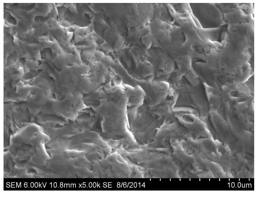
Embodiment 1
[0052] A kind of texturing pretreatment method of diamond wire cut polysilicon chip, comprises the steps:
[0053] (1) Take the polycrystalline silicon chip cut by diamond wire, clean it with a dilute HF solution with a mass concentration of 10%, and dry it, then place the silicon chip in a diffusion furnace, and heat up the diffusion furnace to 880 ° C. Inject large-flow nitrogen gas to remove the gas in the furnace, among which, the flow rate of large-flow nitrogen gas is 800ml / min;
[0054] (2) After the temperature of the diffusion furnace is stabilized, feed nitrogen and oxygen carrying a liquid phosphorus source for diffusion. The diffusion temperature is 880° C., and the diffusion time is 12 minutes. Wherein, the flow rate of nitrogen carrying a liquid phosphorus source is 60ml / min. The flow rate of oxygen is 40ml / min;
[0055] (3) Lead the diffusion furnace into a large flow of nitrogen to complete the diffusion process, and obtain a polysilicon wafer with a phosphoru...
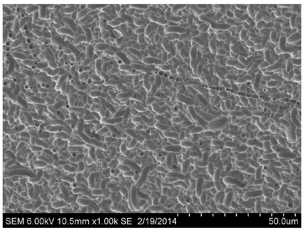
Embodiment 2
[0062] A kind of texturing pretreatment method of diamond wire cut polysilicon chip, comprises the steps:
[0063] (1) Take the polysilicon wafer cut by diamond wire, wash it with a dilute HF solution with a mass concentration of 5%, and dry it, then place the silicon wafer in a diffusion furnace, and heat the diffusion furnace to 850°C, Inject large-flow nitrogen gas to remove the gas in the furnace, among which, the flow rate of large-flow nitrogen gas is 500ml / min;
[0064] (2) After the temperature of the diffusion furnace is stabilized, feed nitrogen and oxygen carrying a liquid phosphorus source for diffusion. The diffusion temperature is 850° C., and the diffusion time is 10 minutes. Wherein, the flow rate of nitrogen carrying a liquid phosphorus source is 40ml / min. The flow rate of oxygen is 30ml / min;
[0065] (3) Leading the diffusion furnace into a large flow of nitrogen gas to complete the diffusion process to obtain a polysilicon wafer with a phosphorus diffusion ...
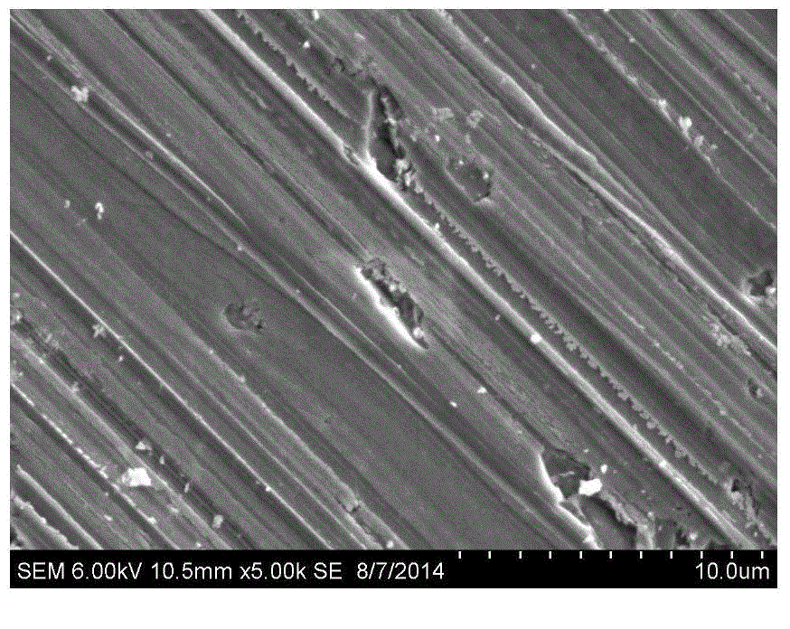
Embodiment 3
[0071] A kind of texturing pretreatment method of diamond wire cut polysilicon chip, comprises the steps:
[0072] (1) Take the polysilicon wafer cut by diamond wire, wash it with a dilute HF solution with a mass concentration of 20%, remove the oil stain and oxide layer on the surface of the silicon wafer, and dry it, then place the silicon wafer in a diffusion furnace , and raise the temperature of the diffusion furnace to 900°C, feed a large flow of nitrogen gas to remove the gas in the furnace, wherein the flow rate of the large flow nitrogen gas is 1000ml / min;
[0073] (2) After the temperature of the diffusion furnace is stabilized, feed nitrogen and oxygen carrying a liquid phosphorus source for diffusion. The diffusion temperature is 900° C., and the diffusion time is 15 minutes. Wherein, the flow rate of nitrogen carrying a liquid phosphorus source is 100 ml / min. The flow rate of oxygen is 90ml / min;
[0074] (3) Leading the diffusion furnace into a large flow of nitr...
PUM
| Property | Measurement | Unit |
|---|---|---|
| reflectance | aaaaa | aaaaa |
| reflectance | aaaaa | aaaaa |
| reflectance | aaaaa | aaaaa |
Abstract
Description
Claims
Application Information