Direct-dimming-type InP-based monolithic integration few-mode optical communication transmitter chip

A single-chip integration and chip technology, applied in the field of optical communication, can solve the problems of sensitive device cost and large demand for optical transceivers, reduce the difficulty and cost of overall manufacturing, reduce the difficulty of chip preparation and the complexity of peripheral circuits, and avoid The effect of complex structures

Active Publication Date: 2015-04-08
INST OF SEMICONDUCTORS - CHINESE ACAD OF SCI
View PDF4 Cites 7 Cited by
  • Summary
  • Abstract
  • Description
  • Claims
  • Application Information

AI Technical Summary

Problems solved by technology

Compared with the backbone network, which is not sensitive to cost, the access network has a large demand for optical transceivers and is sensitive to device cost

Method used


Image

  • Direct-dimming-type InP-based monolithic integration few-mode optical communication transmitter chip
  • Direct-dimming-type InP-based monolithic integration few-mode optical communication transmitter chip
  • Direct-dimming-type InP-based monolithic integration few-mode optical communication transmitter chip

Examples


Embodiment Construction

[0029] In order to make the objectives, technical solutions, and advantages of the present invention clearer, the following further describes the present invention in detail in conjunction with specific embodiments and with reference to the accompanying drawings.

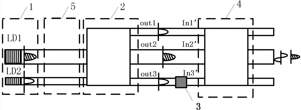
[0030] figure 1 It is a schematic structural diagram of a direct modulation InP-based monolithic integrated few-mode optical communication transmitter chip according to an embodiment of the present invention, such as figure 1 As shown, the directly modulated InP-based monolithic integrated few-mode optical communication transmitter chip includes an InP-based semiconductor laser array 1, a multimode interference power beam splitter 2, a phase shifter 3, a multimode interference mode multiplexer 4, and an optical Waveguide connection structure 5, in which:

[0031] The InP-based semiconductor laser array 1 is used to convert the signal to be transmitted into a modulated fundamental mode optical signal, specifically, the cur...


PUM


Abstract

The invention discloses a direct-dimming-type InP-based monolithic integration few-mode optical communication transmitter chip which comprises an InP-based semiconductor laser array, a multimode interference power beam splitter, an optical waveguide connecting structure, a phase shifter and a multimode interference mode multiplexer. The InP-based semiconductor laser array converts to-be-transmitted signals into basic-mode optical signals, the multimode interference power beam splitter performs beam splitting on the basic-mode optical signals, the optical waveguide connecting structure is connected with the InP-based semiconductor laser array and the multimode interference power beam splitter, the phase shifter performs phase shifting on output of part of output ends of the multimode interference power beam splitter to generate second phase difference between the output of the output ends and output of other output ends and sends signals after phase shifting to the multimode interference mode multiplexer; and the multimode interference mode multiplexer multiplexes the optical signals, converts the basic-mode optical signals of part of lasers in the InP-based semiconductor laser array into an order mode and performs multiplexing output on the basic-mode optical signals together with the basic-mode optical signals of other lasers. By the chip, manufacturing difficulty and cost of devices and modules are lowered, and large-scale application of mode splitting multiplexing technology on a level of an access network is facilitated.

Description

Technical field [0001] The invention relates to the technical field of optical communication, in particular to a direct-adjusted InP-based monolithic integrated few-mode optical communication transmitter chip, which is applied in a short- and medium-distance few-mode optical fiber communication system. Background technique [0002] With the commercialization of 100G, people's requirements for data network capacity continue to rise. The methods currently used to improve communication capacity are mainly based on the improvement of single-mode fiber spectrum efficiency, such as dense wavelength division multiplexing, optical time division multiplexing, polarization multiplexing, and new coding modulation technologies. However, recent studies have shown that with the adoption of smaller channel spacing and higher modulation formats, the inherent nonlinearity of single-mode fiber and the ASE noise of the amplifier have made the system capacity closer to the Shannon limit. [0003] In ...

Claims


Application Information

Patent Timeline
Patent Type & Authority Applications(China)
IPC IPC(8): G02B6/42
CPCG02B6/4215
Inventor 张莉萌陆丹赵玲娟余力强潘碧玮王圩
Owner INST OF SEMICONDUCTORS - CHINESE ACAD OF SCI
Why Eureka
Try Eureka