Aluminum etching technology of thin field aluminum gate and application thereof
A technology of aluminum etching and aluminum gate, which is applied in the direction of semiconductor devices, etc., can solve the problems of difficult thin field aluminum gate aluminum etching, gate oxide is easy to be etched through, and aluminum oxide layer is low, so as to achieve good uniformity and avoid Effects of damaging the substrate and increasing the flow rate of chlorine gas
- Summary
- Abstract
- Description
- Claims
- Application Information
AI Technical Summary
Problems solved by technology
Method used
Image
Examples
Embodiment 1
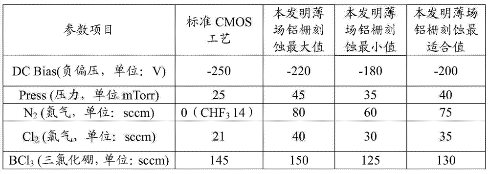
[0070] The aluminum etching process of the thin-field aluminum grid in this embodiment is carried out using an Applied Materials 8330 aluminum etching machine, and the aluminum etching conditions of the thin-field aluminum grid are as follows:
[0071] Main etch:
[0072] 30 sccm Cl 2 / 150sccm BCl 3 / 35mTorr / -180V / EPD;
[0073] Over etch:
[0074] 30 sccm Cl 2 / 150sccm BCl 3 / 35mTorr / -180V / 01:00.
[0075] It is found through experiments that the etching process of this embodiment has better uniformity and higher selectivity than the standard CMOS process. The specific results are shown in Table 2, where the selection ratio (Al / PR) represents the selection ratio of aluminum to photoresist.
[0076] Table 2: Comparison of the effects of the etching process in Example 1 and the standard CMOS process
[0077] craft
Intra-chip uniformity
Uniformity between slices
Select ratio (Al / OX)
Selection ratio (Al / PR)
Standard CMOS process
10%
1...
Embodiment 2
[0082] The aluminum etching process of the thin-field aluminum grid in this embodiment is carried out using an Applied Materials 8330 aluminum etching machine, and the aluminum etching conditions of the thin-field aluminum grid are as follows:
[0083] Main etch:
[0084] 40sccm Cl 2 / 130sccm BCl 3 / 45mTorr / -220V / EPD;
[0085] Over etch:
[0086] 40sccm Cl 2 / 130sccm BCl 3 / 45mTorr / -220V / 01:00.
[0087] It is found through experiments that the etching process of this embodiment has better uniformity and higher selectivity than the standard CMOS process. The specific results are shown in Table 4.
[0088] Table 4: Comparison of the effects of the etching process in Example 2 and the standard CMOS process
[0089] craft
Intra-chip uniformity
Uniformity between slices
Select ratio (Al / OX)
Selection ratio (Al / PR)
Standard CMOS process
10%
10%
2.5:1
1.4:1
Embodiment 2 etching process
8%
8%
9:1
1.6:1
...
Embodiment 3
[0094] The process of this embodiment is carried out using an Applied Materials 8330 aluminum etching machine, and the aluminum etching conditions of the thin-field aluminum grid are as follows:
[0095] Main etch: 35sccm Cl 2 / 130sccm BCl 3 / 40mTorr / -200V / EPD;
[0096] Overetch: 35sccm Cl 2 / 130sccm BCl 3 / 40mTorr / -200V / 01:00.
[0097] It is found through experiments that the etching process of this embodiment has better uniformity and higher selectivity than the standard CMOS process. The specific results are shown in Table 6.
[0098] Table 6: Comparison of the effects of the etching process in Example 3 and the standard CMOS process
[0099] craft
Intra-chip uniformity
Uniformity between slices
Select ratio (Al / OX)
Selection ratio (Al / PR)
Standard CMOS process
10%
10%
2.5:1
1.4:1
Embodiment 3 etching process
7%
8%
8:1
1.5:1
[0100] In the application material 8330 etching process of this ...
PUM
 Abstract
Description
Claims
Application Information


