

Depletion channel super-barrier rectifier and manufacturing method thereof
A super-barrier rectifier, depletion-type technology, applied in the manufacture of depletion-type channel super-barrier rectifiers, depletion-type channel super-barrier power rectifier field, can solve the problem of affecting forward conduction voltage drop, high turn-on Voltage, rectifier temperature rise and other issues, to achieve the effect of enhancing controllability, good high temperature stability, and reducing production costs
- Summary
- Abstract
- Description
- Claims
- Application Information
AI Technical Summary
Problems solved by technology
Method used
Image

Examples
Embodiment 1
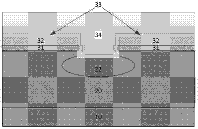
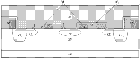
[0039] Such as figure 2 As shown, a depletion-type channel super-barrier rectifier includes a heavily doped first conductivity type substrate 10, a lightly doped first conductivity type drift region 20, a second conductivity type body region 22, and a field dielectric layer 30 , gate dielectric layer 31 , polysilicon layer 32 , compound metal layer 33 and metal layer 34 . Typical parameters are selected as follows: the heavily doped first conductivity type substrate 10 is N-type doped with a concentration greater than the 19th power, the lightly doped first conductivity type drift region 20 is N-type doped with a medium doping concentration, The second conductivity type body region 22 is P-type doped with medium doping concentration, the field dielectric layer 30 is silicon dioxide with a thickness of 5000A to 10000A, and the gate dielectric layer 31 is thermally grown silicon dioxide with a thickness of 50A to 100A. The compound metal layer comes from the silicide formed af...
Embodiment 2
[0049] This embodiment discloses a method for manufacturing a depletion-type trench super-barrier rectifier, including the following steps:
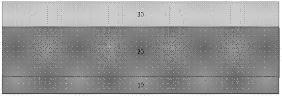
[0050] 1) as image 3 As shown, a lightly doped first conductive type drift region 20 is covered on a heavily doped first conductive type substrate 10, and a field dielectric layer 30 is formed on the lightly doped first conductive type drift region 20, thereby as the basis for the device.
[0051] 2) such as Figure 4 As shown, a mask layer 35 is covered on the field dielectric layer 30 . The mask layer 35 has an annular through groove. The field dielectric layer 30 below the annular through groove of the mask layer 35 is etched so that the annular through groove is formed on the field dielectric layer 30 , and the mask layer 35 is removed. The bottom of the annular channel on the field dielectric layer 30 is the lightly doped drift region 20 of the first conductivity type.
[0052] 3) as Figure 5 As shown, the lightly doped drif...
PUM
 Abstract
Description
Claims
Application Information