Graphene field effect transistor structure and large-scale manufacturing process thereof

A field-effect transistor and manufacturing process technology, which is applied in semiconductor/solid-state device manufacturing, semiconductor devices, electrical components, etc., can solve problems such as high process difficulty, poor performance, and low yield rate, and achieve the effect of overcoming high process difficulty

Active Publication Date: 2015-04-22
广西北部湾粮油技术研究有限公司
View PDF4 Cites 8 Cited by
  • Summary
  • Abstract
  • Description
  • Claims
  • Application Information

AI Technical Summary

Problems solved by technology

[0003] Purpose of the invention: In order to overcome the deficiencies in the prior art, the present invention provides a graphene field effect transistor structure, which overcomes the problems of high tec

Method used


Image

  • Graphene field effect transistor structure and large-scale manufacturing process thereof

Examples


Embodiment Construction

[0027] The present invention will be further described below in conjunction with the accompanying drawings.

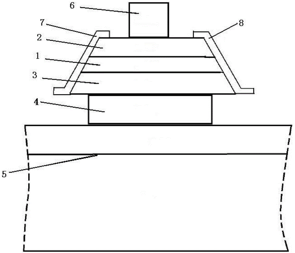
[0028] h-BN is a dielectric material with a band gap of about 5.9eV. Its lattice structure is very similar to graphene, and its surface is also a two-dimensional planar structure. There are no surface dangling bonds and internal charged defects. Graphene is an ideal substrate material. And because the lattice mismatch between h-BN and graphene is small, and the surface is smooth without dangling bonds, the carrier mobility of field effect transistors using h-BN as gate dielectric is higher than that of traditional SiO2 or A field effect transistor with SiC as the substrate and Al2O3 as the gate dielectric. Edge contact, namely 1D contact, is a technology that deposits wires on the edge of the channel material to achieve electrical contact. Graphene lacks surface binding sites, and the strong orbital hybridization and (and intermetallic) lack of chemical bonding in it...


PUM


Abstract

The invention discloses a graphene field effect transistor structure and a large-scale manufacturing process of the graphene field effect transistor structure. The manufacturing process comprises the steps that firstly, selective growing is carried out on a bottom h-BN dielectric layer and a graphene layer on a catalytic metal thin film layer according to the characteristic of the catalytic metal thin film layer, then photoetching is carried out on the catalytic metal thin film layer, the shape of the bottom h-BN dielectric layer and the graphene layer growing epitaxially is controlled, and finally two-time photoetching on the catalytic metal thin film layer and growing of a top grid h-BN dielectric layer are achieved through structure inversion and connection of two times. The structure comprises the bottom h-BN dielectric layer, the graphene layer and the top grid h-BN dielectric layer, the bottom h-BN dielectric layer, the graphene layer and the top grid h-BN dielectric layer are sequentially arranged from bottom to top, a grid electrode is arranged on the top grid h-BN dielectric layer, and a source electrode and a drain electrode are guided out of the two sides of the graphene layer. According to the graphene field effect transistor structure and the manufacturing process, the problem that an existing process is high in difficulty, low in rate of finished products and poor in product performance is solved, and a good foundation is laid for manufacturing of a graphene-based integrated circuit.

Description

technical field [0001] The invention belongs to the field of semiconductor devices and semiconductor technology. Background technique [0002] Graphene is a two-dimensional material with extremely excellent performance formed by carbon atoms in a hexagonal honeycomb lattice. Its carrier velocity and mobility are much higher than conventional semiconductor materials. It is considered as an integrated circuit material in the post-silicon era. Currently, large-scale graphene wafers can be grown by CVD on catalytic metal substrates and SiC epitaxy. When preparing graphene electronic devices, either the graphene prepared by CVD method needs to be transferred to two SiO / Si (or other) substrates, or the 6H-SiC substrate is directly used as the dielectric layer. These substrates not only The surface has a certain roughness, and there are high-density Coulomb centers in it, coupled with the scattering of optical phonons in the substrate material, the carrier mobility in graphene wil...

Claims


Application Information

Patent Timeline
IPC IPC(8): H01L29/78H01L21/336
CPCH01L29/408H01L29/66477H01L29/78
Inventor 邱祖全
Owner 广西北部湾粮油技术研究有限公司
Why Eureka
Try Eureka