A nanoplasma array laser and its manufacturing method

A plasma and nanowire array technology, which is applied in the field of plasma array lasers and its production, can solve the problems of no device formation, irregular growth of nanowire arrays, and limited laser power, and achieve the effect of increasing laser power

Inactive Publication Date: 2017-05-10
UNIV OF ELECTRONICS SCI & TECH OF CHINA
View PDF6 Cites 0 Cited by
  • Summary
  • Abstract
  • Description
  • Claims
  • Application Information

AI Technical Summary

Problems solved by technology

However, it has the following disadvantages: 1) the nanowire is single, which limits the power of the laser; 2) the pumping method is pulsed laser pumping, which will greatly increase the size of the laser in practical applications; 3) the working temperature is less than 10K Ultra-low temperature, not conducive to practical application
[0004] The manufacturing process of the electrically pumped semiconductor nanowire array laser is: prepare an n-type zinc oxide (ZnO) film on the substrate, and grow a p-type ZnO nanowire (hexagonal prism) array doped with antimony (Sb) on the n-type ZnO film At room temperature, electrodes are made on the substrate and the top of the nanowires for electrical pumping, and the laser is emitted from the top of the nanowires; its disadvantages are also very obvious: 1) The growth of nanowire arrays is irregular, which is not conducive to the synthesis of beams and power ; 2) Beam synthesis is not performed, laser packaging is not completed, and no device is formed
[0005] Research on nano-lasers based on zinc oxide, cadmium sulfide and other materials has attracted widespread attention from scientists. By introducing semiconductor nanowires or nano-arrays, micro-lasers and nano-lasers have reached the level of the diffraction limit, but due to the existence of the diffraction limit, semiconductor nano-lasers have been limited. Laser Minimum Size

Method used


Image

  • A nanoplasma array laser and its manufacturing method
  • A nanoplasma array laser and its manufacturing method
  • A nanoplasma array laser and its manufacturing method

Examples


Embodiment

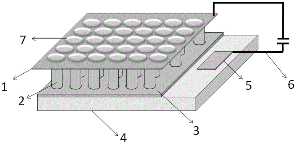
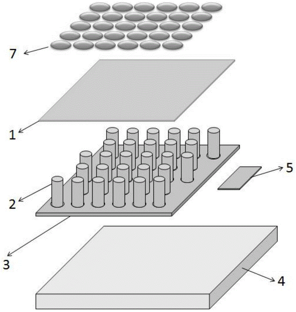
[0036] This embodiment provides a nanoplasma array laser, the structure of which is as follows figure 1 as shown, figure 2 is a schematic diagram of its structural disassembly, the nanowire array is composed of 19 coherent light sources, such as Figure 5 As shown, each coherent light source is identical, and the working mode is TEM 00 Die, some specific materials, parameters and dimensions are as follows:

[0037] The semiconductor substrate 4 is a gallium nitride (GaN) substrate;

[0038] The insulating dielectric layer 3 is SiO 2 Thin film layer, its thickness is 300nm;

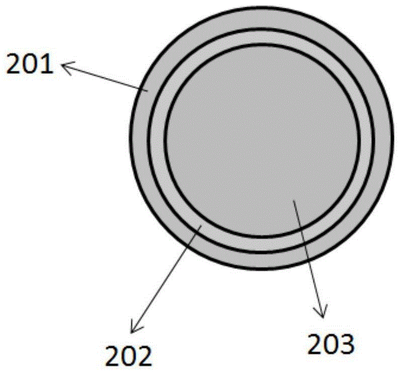
[0039] The SiO 2 The film layer 3 is provided with a circular through-hole array arranged in a hexagonal close-packed array, such as Figure 4 As shown, the diameter of the through hole is 200nm, and the distance between the centers of adjacent through holes is 1 μm; ZnO nanowires 203 are grown at each position of the through hole, and the length thereof is 3 μm;

[0040] The sides of the ZnO nanow...


PUM


Abstract

The invention provides a nano-plasma array laser and a manufacturing method thereof, belonging to the field of optical technology. The invention utilizes the interaction between the photons excited by the p-n junction array of electrically pumped semiconductor nanowires and the surface metal-dielectric film to generate surface plasmon polaritons (SPPs), and then constrains and regulates the photon beams generated in the nanowire resonant cavity . The present invention combines the dual advantages of geometric limitation of semiconductor nanostructures and surface plasmon mode field constraints on light beams, uses semiconductor nanowires to realize the integration of working materials and resonant cavities and surface plasmons to achieve mode field constraints, and finally forms a semiconductor nanoplasma laser .

Description

technical field [0001] The invention belongs to the field of optical technology, and in particular relates to a nano-plasma array laser and a manufacturing method thereof. Background technique [0002] Since the first laser was produced 50 years ago, some new nanotechnology has improved the micro-laser to a new field, which has set off a research boom of nano-laser. At present, the widely used nanolasers mainly include optically pumped nanoplasmonic lasers and electrically pumped semiconductor nanowire array lasers. [0003] Optically pumped nanoplasmonic laser consists of a single semiconductor cadmium sulfide (CdS) nanowire placed horizontally on a metal-dielectric composite film to form a nanoplasmonic laser, and laser emission is achieved through pulsed laser pumping; The nano-scale slit realizes the surface plasmon local field enhancement effect for plasmon-optical hybrid pumping, and realizes laser emission at the end of the nanowire. The excitation light mode is rest...

Claims


Application Information

Patent Timeline
Patent Type & Authority Patents(China)
IPC IPC(8): H01S5/04H01S5/20
Inventor 赵青黄小平刘友亮王鹏
Owner UNIV OF ELECTRONICS SCI & TECH OF CHINA
Why Eureka
Try Eureka