

One-step type manufacturing method for silicon-dioxide-based diffraction grating
A technology of diffraction grating and silicon dioxide, which is applied in the direction of diffraction grating, photographic plate-making process of pattern surface, optics, etc., can solve the problems that have not been reported in the field of precision optical instrument manufacturing, and achieve shortening of production cycle, reduction of production cost, Effects of Accuracy and Resolution Improvement
- Summary
- Abstract
- Description
- Claims
- Application Information
AI Technical Summary
Problems solved by technology
Method used
Image

Examples
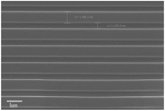
Embodiment 1
[0030] The nanoimprinting equipment used in the embodiment is SUSS MicroTec-SCIL, the lithography equipment is SUSS MA6 lithography machine, nanoimprinting glue: purchased from Philips in the Netherlands, the label is: SOL-GEL V5-500;
[0031] The predetermined thickness of the nano-imprint adhesive of spin coating in the embodiment is 500nm;
[0032] Taking the production of a high-quality diffraction grating with sub-micron parallel equal width and equal spacing as an example, the production steps are as follows:
[0033] Step 1: Install the nano-imprint element equipment on the lithography machine, change the working mode of the lithography machine to be in the nano-imprint mode, and then place the soft template whose working surface matches the shape of the grating to be processed on the nano-imprint On the stencil mask of the device and vacuum fixed;
[0034] Step 2: Pretreat the silicon substrate used, first ultrasonic cleaning with acetone for 15 minutes, then ultrason...
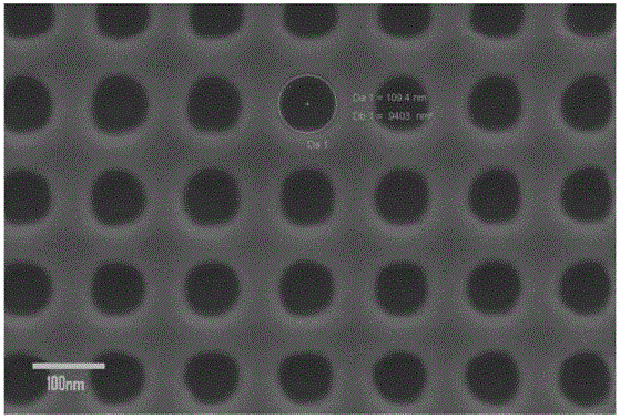
Embodiment 2
[0045]The nanoimprinting equipment used in the embodiment is SUSS MicroTec-SCIL, the lithography equipment is SUSS MA6 lithography machine, nanoimprinting glue: purchased from Philips in the Netherlands, the label is: SOL-GEL V5-500;
[0046] The predetermined thickness of the nano-imprint adhesive of spin coating in the embodiment is 500nm;
[0047] Taking a diffraction grating with periodic regular holes on the submicron scale as an example, the fabrication steps are as follows:
[0048] Step 1: Install the nano-imprint element equipment on the lithography machine, change the working mode of the lithography machine to be in the nano-imprint mode, and then place the soft template whose working surface matches the shape of the grating to be processed on the nano-imprint On the stencil mask of the device and vacuum fixed;
[0049] Step 2: Pretreat the silicon substrate used, first ultrasonic cleaning with acetone for 15 minutes, then ultrasonic cleaning with ethanol for 15 min...
PUM
 Abstract
Description
Claims
Application Information