Forming method of silicon through hole

A through-silicon via, ring-shaped technology, used in electrical components, semiconductor/solid-state device manufacturing, circuits, etc., can solve problems such as large differences in thermal expansion coefficients, reduced reliability of through-silicon vias, and delamination of conductive layers and diffusion barrier layers. , to achieve the effect of improving reliability and reducing the possibility of delamination and cracking

Active Publication Date: 2015-04-29
SEMICON MFG INT (SHANGHAI) CORP
View PDF5 Cites 9 Cited by
  • Summary
  • Abstract
  • Description
  • Claims
  • Application Information

AI Technical Summary

Problems solved by technology

[0004] However, in the TSVs fabricated by existing methods, the conductive layer and the diffusion barrier layer in the TSVs are prone to delamination or cracking. There are two reasons for these phenomena: on the one hand, the diffusion barrier layer and the diffusion barrier layer There is a thermal mismatch between the conductive layers, that is, the difference in thermal expansion coefficient between the two is relatively large; on the other hand, the conductive layer in the existing TSV fills the entire through hole, so the gap between the conductive layer and the diffusion barrier layer greater stress
The phenomenon of delamination or cracking in the diffusion barrier layer will cause the material of the conductive layer to diffuse into the semiconductor substrate around the TSV, resulting in a decrease in the reliability of the TSV.
[0005] Therefore, a new method for forming TSVs is needed to solve the problem that the diffusion barrier layer in the existing TSVs is prone to delamination or cracking.

Method used


Image

  • Forming method of silicon through hole
  • Forming method of silicon through hole
  • Forming method of silicon through hole

Examples


Embodiment Construction

[0037] Existing methods for forming TSVs generally include:

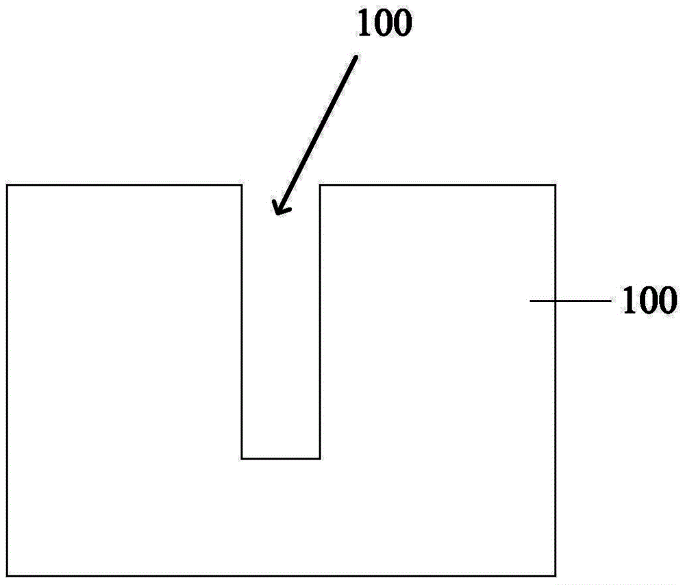
[0038] like figure 1 As shown, a semiconductor substrate 100 is provided, and a via hole 101 is formed on the semiconductor substrate 100;

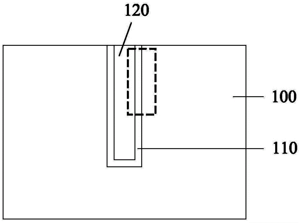
[0039] like figure 2 shown in figure 1 A diffusion barrier layer 110 is formed on the surface of the via hole 101 shown, and a metal layer 120 is continuously filled in the via hole 101. The material of the metal layer 120 may be copper, and then planarized to obtain a through silicon via.

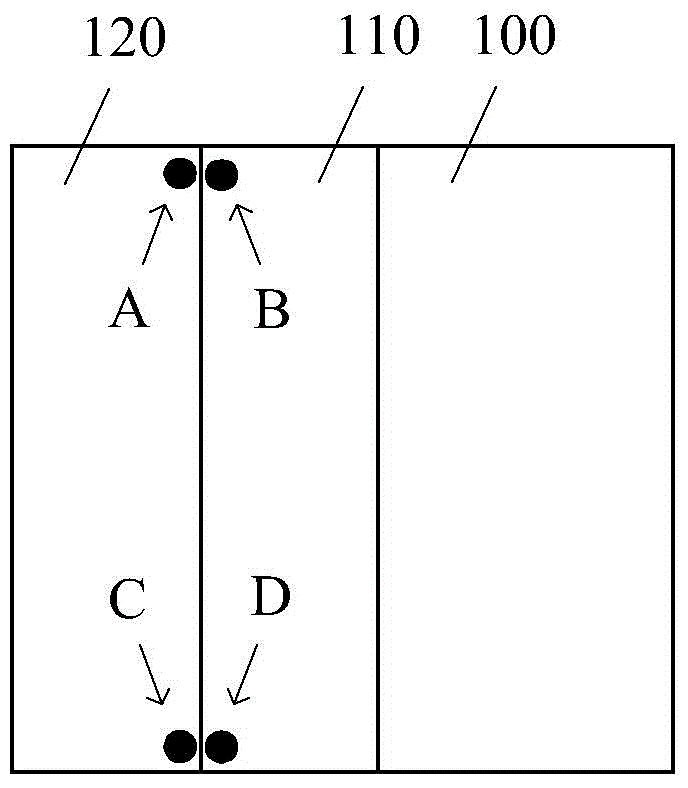
[0040] image 3 for figure 2 In the shown structure, it is an enlarged schematic view of the part surrounded by the dotted line box, and the part surrounded by the dotted line box includes a part of the metal layer 120 , a part of the diffusion barrier layer 110 and a part of the semiconductor substrate 100 arranged in sequence. exist image 3 Points A, B, C and D are selected from the shown TSVs. Point A and point B are located at the top of the TSV, and point A is located in th...


PUM


Abstract

The invention relates to a forming method of a silicon through hole. The forming method comprises the following steps: providing a semiconductor substrate; forming a ring-shaped through hole in the semiconductor substrate, wherein the semiconductor substrate inside the ring-shaped through hole is an isolated semiconductor pillar; forming diffusion barrier layers on the side wall and at the bottom of the ring-shaped through hole; full filling the ring-shaped through hole with a conductive layer; removing all the semiconductor pillar or removing part of the semiconductor pillar to reserve part of a thickness until an opening with a depth-to-width ratio of greater than or equal to 20 is formed; and sealing the opening to form an air gap. According to the method, firstly the ring-shaped through hole is formed, the ring-shaped through hole is full filled with the conductive layer, then the semiconductor pillar formed inside the ring-shaped through hole in a surrounding manner is removed to form the opening and the opening is sealed to form the air gap; the air gap provides a large deformation space for plastic deformation of the conductive layer and is beneficial for releasing stresses in the conductive layer and an insulating layer; the possibility that a silicon through hole generates the layering and cracking phenomena is reduced; and reliability of the silicon through hole is improved.

Description

technical field [0001] The invention relates to the technical field of semiconductors, in particular to a method for forming through-silicon holes. Background technique [0002] With the continuous development of semiconductor technology, the feature size of semiconductor devices has become very small. It is becoming more and more difficult to increase the number of semiconductor devices in a two-dimensional packaging structure. Therefore, three-dimensional packaging has become a method that can effectively improve chip integration. degree method. Current three-dimensional packaging includes die stacking based on wire bonding, package stacking and three-dimensional stacking based on through silicon vias (Through Silicon Via, TSV). [0003] The three-dimensional stacking technology based on through-silicon vias has the following three advantages: (1) high-density integration; (2) greatly shortening the length of electrical interconnections, which can well solve the problems ...

Claims


Application Information

Patent Timeline
Patent Type & Authority Applications(China)
IPC IPC(8): H01L21/768
CPCH01L21/768H01L21/76898
Inventor 沈哲敏李广宁
Owner SEMICON MFG INT (SHANGHAI) CORP
Why Eureka
Try Eureka