

Manufacturing method for metal interconnecting structure
A technology of metal interconnection structure and manufacturing method, applied in semiconductor/solid-state device manufacturing, electrical components, circuits, etc. The etching process is easy, the thickness of the photoresist is reduced, and the effect of resisting large currents is improved
- Summary
- Abstract
- Description
- Claims
- Application Information
AI Technical Summary
Problems solved by technology
Method used
Image

Examples
Embodiment Construction
[0031] Such as figure 2 Shown is a flowchart of a method for manufacturing a metal interconnection structure according to an embodiment of the present invention; as Figure 3A to Figure 3H Shown is a schematic diagram of the metal interconnection structure in each step of the method of the embodiment of the present invention. The manufacturing method of the metal interconnection structure according to the embodiment of the present invention includes the following steps:
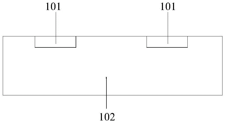
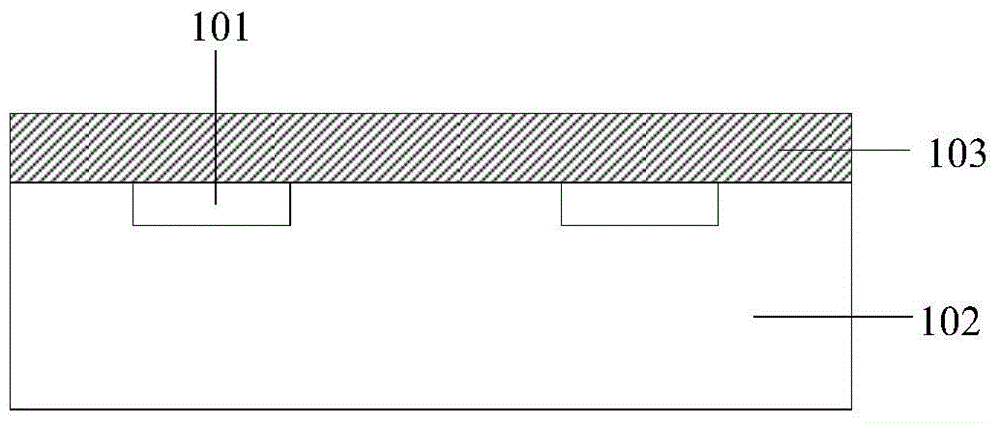
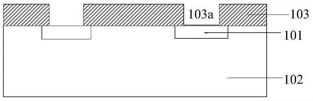
[0032] Step 1, such as Figure 3A As shown, a substrate 2 is provided, on which a doped region 1 that needs to be drawn out through a metal interconnection structure is formed, and the doped region 1 is formed by implantation or diffusion. Such as Figure 3B As shown, after the final implantation and diffusion are completed, a dielectric layer 3 is grown or deposited on the substrate 2, and the dielectric layer 3 serves as an interlayer film.
[0033] Preferably, the dielectric layer 3 is an oxide dielec...
PUM
| Property | Measurement | Unit |
|---|---|---|
| thickness | aaaaa | aaaaa |
| width | aaaaa | aaaaa |
Abstract
Description
Claims
Application Information