
Eureka
For R&D, Eureka makes reading and utilizing patents & technical documents easy.
Eureka AIR
Designed for self-driven R&D workflows. Generate viable solutions, solve complex R&D challenges, empower your innovation with AI.

Eureka Materials
Designed for material experts only. Revolutionize your material R&D, from search, analyze, to developing new materials.

TechResearch
Generate reliable direction feasibility study reports for your R&D in just a few steps.

TechSeek
Discover and master advanced knowledge NOW. Basics, ideas, possibilities, all at once.

TechMind
As an expert in R&D Theories, TechMind can generates customized viable solutions instantly.

TechRisk
Analyze your overall solution with one click, know your potential R&D risks in advance.

TechMonitor
Get weekly tech updates, stay abreast of the latest tech innovations and key insights.
Packaging convex point structure
A bump structure and layer structure technology, applied in electrical components, electric solid devices, circuits, etc., can solve problems such as bumps prone to microcracks, affect welding quality, and large internal stress, and improve long-term stability and reliability. performance, low cost, and the effect of reducing internal stress
- Summary
- Abstract
- Description
- Claims
- Application Information
AI Technical Summary
Problems solved by technology
Method used
Image

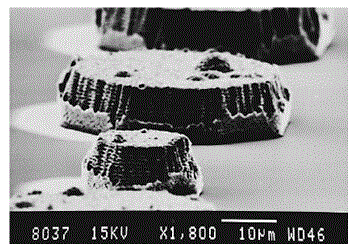
Examples
Embodiment Construction
[0033] The present invention will be further described below in conjunction with accompanying drawing:
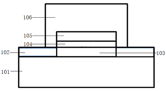
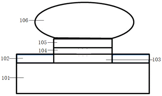
[0034] Such as figure 1 A bump structure for packaging shown includes a substrate layer 101 , a passivation layer 102 , a pad layer 103 , an adhesive layer 104 , a composite solder resist wetting layer 105 and a pre-solder layer 106 .
[0035] Both the passivation layer 102 and the pad layer 103 are located above the substrate layer 101 , and an opening is provided above the passivation layer 102 , and the pad layer 103 is embedded in the opening of the passivation layer 102 . The adhesive layer 104 , the composite solder resist wetting layer 105 , and the pre-solder layer 106 are sequentially arranged above the pad layer 103 from bottom to top.
[0036] The substrate layer 101 as the support of the entire bump structure should have good mechanical strength and good long-term stability. The material of the substrate layer is alumina ceramics, aluminum nitride ceramics, lo...
PUM
| Property | Measurement | Unit |
|---|---|---|
| Thickness | aaaaa | aaaaa |
| Surface roughness | aaaaa | aaaaa |
| Flatness | aaaaa | aaaaa |
Abstract
Description
Claims
Application Information
 - R&D Engineer
- R&D Manager
- IP Professional
- Industry Leading Data Capabilities
- Powerful AI technology
- Patent DNA Extraction
Browse by: Latest US Patents, China's latest patents, Technical Efficacy Thesaurus, Application Domain, Technology Topic, Popular Technical Reports.
© 2024 PatSnap. All rights reserved.Legal|Privacy policy|Modern Slavery Act Transparency Statement|Sitemap|About US| Contact US: help@patsnap.com