OTP (one-time programmable memory) device and manufacturing method thereof

A manufacturing method and device technology, which can be used in semiconductor/solid-state device manufacturing, electric solid-state devices, semiconductor devices, etc., can solve problems such as the reduction of memory area, and achieve the effect of improving compatibility

Active Publication Date: 2015-04-29
SHANGHAI HUAHONG GRACE SEMICON MFG CORP
View PDF6 Cites 2 Cited by
  • Summary
  • Abstract
  • Description
  • Claims
  • Application Information

AI Technical Summary

Problems solved by technology

Compared with the existing first OTP device, the existing second OTP device has a large reduction in the memory area; but because the floating gate is used as the electronic memory, the data storage capacity must have a certain limit for the thickness of the gate oxide film. As the requirements of NVM data storage, the theoretical value of the gate oxide film thickness is required to be above 60A, which is greater than the thickness of the gate oxide film used in the standard CMOS process. In this way, OTP is limited as an embedded part of the standard CMOS process. use

Method used


Image

  • OTP (one-time programmable memory) device and manufacturing method thereof
  • OTP (one-time programmable memory) device and manufacturing method thereof
  • OTP (one-time programmable memory) device and manufacturing method thereof

Examples


Embodiment Construction

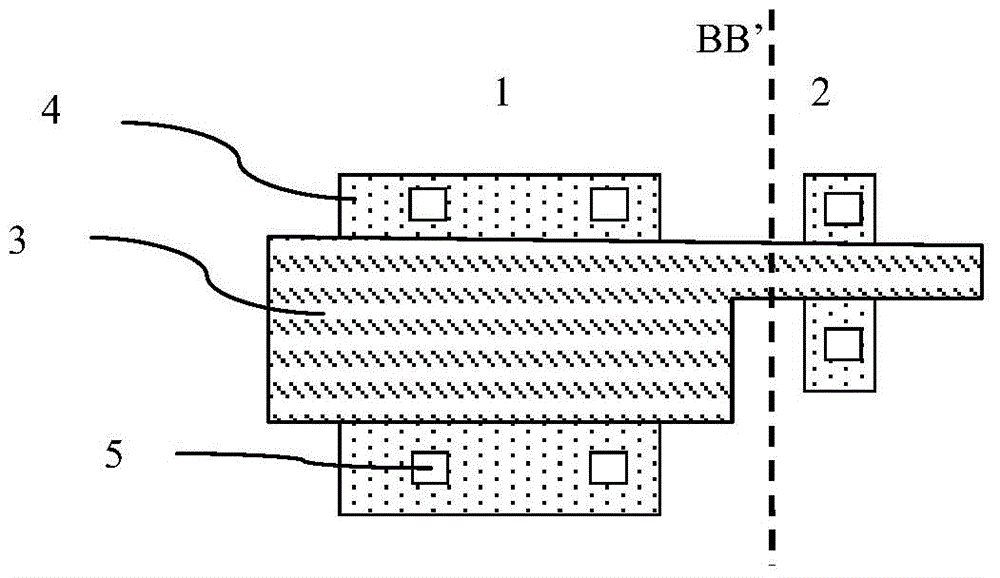
[0044] Such as image 3 Shown is a schematic structural diagram of an OTP device according to an embodiment of the present invention. The unit structure of the OTP device in the embodiment of the present invention includes a PMOS transistor and a PNPN thyristor.

[0045] The PMOS transistors include:

[0046] The N well 2 is formed in the semiconductor substrate 1 , and the N well 2 extends downward to a certain depth from the top surface of the semiconductor substrate 1 . Preferably, the semiconductor substrate 1 is a silicon substrate.

[0047] The gate structure includes a gate dielectric layer 3 and a polysilicon gate 4 sequentially formed above the semiconductor substrate 1; the surface of the N well 2 covered by the gate structure is used to form a channel region. Preferably, the gate dielectric layer 3 is a gate oxide layer.

[0048] P+ doped source region 7b and drain region 7a formed in the surface region of the N well 2, the surface region of the N well 2 is also...


PUM


Abstract

The invention discloses an OTP (one-time programmable memory) device which comprises a PMOS (p-channel metal oxide semiconductor) transistor and a PNPN thyristor, wherein the PNPN thyristor is positioned on the source region side of the gate structure of the PMOS transistor; a first P+ doped regions and a source region of the PNPN thyristor are shared, and a first N+ doped region is positioned between two P+ doped regions and in lateral contact with the P+ doped regions; the cathode, the anode and the control electrode of the PNPN thyristor are led out of an N well, the first P+ doped region and a second P+ doped region respectively, and a bit line is led out of the first N+ doped region; the state of the OTP device is determined through whether thermal breakdown between the first P+ doped region and the first N+ doped region is formed or not. The invention further discloses a manufacturing method for the OTP device. According to the OTP device and the manufacturing method, the device area can be reduced, so that the integration level of the device is increased and the compatibility between the device and a CMOS (complementary metal oxide semiconductor) process can be improved; programming current is relatively small, so that programming can be carried out by current pulses generated by circuits, without externally applied current pulses.

Description

technical field [0001] The present invention relates to the field of semiconductor integrated circuit manufacturing, in particular to a one-time programmable (one-time programmable memory, OTP) device; the present invention also relates to a manufacturing method of the OTP device. Background technique [0002] OTP device is a common non-volatile memory (NVM), which has more applications in embedded NVM with limited density and limited performance. Traditional electrically erasable programmable read-only memory (EEPROM), S0NOS, embedded flash memory (E-Flash) NVM is expensive. OTP devices and CMOS-compatible embedded NVM technology is a successful solution in the current industry, and has been widely used in applications such as analog technology trimming from the bit level to the kilobit level of data or code storage. . [0003] There are many types of structural designs of OTP memory cells. There are mainly two types of representative ones: [0004] Such as Figure 1A S...

Claims


Application Information

Patent Timeline
Patent Type & Authority Applications(China)
IPC IPC(8): H01L27/115G11C16/04H01L21/8247
Inventor 郭振强
Owner SHANGHAI HUAHONG GRACE SEMICON MFG CORP
Why Eureka
Try Eureka