Short wave/medium wave/long wave infrared detector based on InAs/GaSb class II-type superlattice materials

An infrared detector and superlattice technology, applied in semiconductor devices, electrical components, circuits, etc., can solve problems such as limiting the application range of detector bias voltage, and achieve the goal of suppressing tunneling dark current, improving quantum efficiency, and suppressing crosstalk Effect

Active Publication Date: 2015-04-29
HARBIN INST OF TECH
View PDF2 Cites 33 Cited by
  • Summary
  • Abstract
  • Description
  • Claims
  • Application Information

AI Technical Summary

Problems solved by technology

[0004] Currently, crosstalk between signal channels in different bands is a major problem for polychromatic infrared detectors, which limits the range of detector bias applications

Method used


Image

  • Short wave/medium wave/long wave infrared detector based on InAs/GaSb class II-type superlattice materials
  • Short wave/medium wave/long wave infrared detector based on InAs/GaSb class II-type superlattice materials

Examples


Embodiment Construction

[0030] The technical solution of the present invention will be further described below in conjunction with the accompanying drawings, but it is not limited thereto. Any modification or equivalent replacement of the technical solution of the present invention without departing from the spirit and scope of the technical solution of the present invention should be covered by the present invention. within the scope of protection.

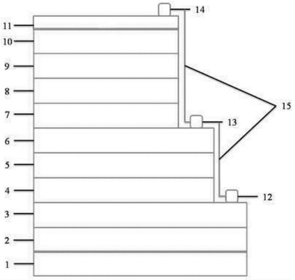
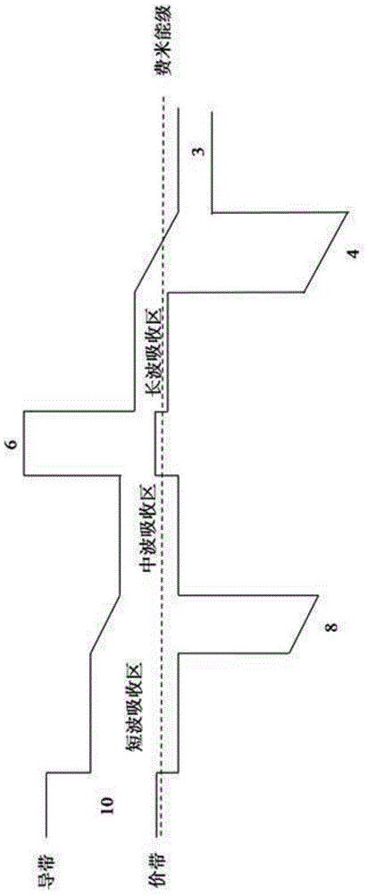
[0031] Based on the particularity of the energy band of the M-type superlattice barrier layer, the invention can significantly suppress the generation-recombination dark current in the depletion layer and the tunneling dark current in the center of the trap, thereby enhancing the photocurrent and realizing the detection rate of the detector D. * The improvement; the existence of the M-type superlattice barrier layer can well suppress the crosstalk between different signals when the signal is extracted by modulating the bias voltage.

[0032] Such as f...


PUM


Abstract

The invention discloses a short wave/medium wave/long wave infrared detector based on InAs/GaSb class II-type superlattice materials. The detector comprises a GaSb substrate, an epitaxial structure deposited on the GaSb substrate, a passivation layer and a metal electrode, wherein the epitaxial structure sequentially comprises a GaSb buffering layer, an n-type InAs/GaSb superlattice contact layer, a first M-type InAs/GaSb/AlSb/GaSb/InAs superlattice hole blocking layer, a p-type InAs/GaSb superlattice long wave infrared absorbing layer, a first p-type InAs/GaSb superlattice contact layer, a p-type InAs/GaSb superlattice medium wave infrared absorbing layer, a second M-type InAs/GaSb/AlSb/GaSb/InAs superlattice hole blocking layer, a p-type InAs/GaSb superlattice short wave infrared absorbing layer, a second p-type InAs/GaSb superlattice contact layer and a cover layer. The detector is of a pMp-p-pi-M-n heterostructure and has the advantages of being low in crosstalk, low in dark current and high in detection rate.

Description

technical field [0001] The invention belongs to the technical field of semiconductors, and relates to a three-color infrared detector based on InAs / GaSb II short-wave (1-3 μm) / medium-wave (3-5 μm) / long-wave (8-14 μm). Background technique [0002] Infrared detectors are widely used in military and civilian fields such as strategic early warning, tactical alarm, night vision, guidance, communication, meteorology, earth resource detection, industrial flaw detection, medicine, spectrum, temperature measurement, and atmospheric monitoring. With the development of detection technology and the improvement of detection effect requirements, the current infrared detection technology is developing towards the direction of obtaining more target information. At present, one of the important development directions of the third-generation infrared detectors at home and abroad is to realize multi-band simultaneous detection. If a detection system can obtain target information in multiple ...

Claims


Application Information

Patent Timeline
Patent Type & Authority Applications(China)
IPC IPC(8): H01L31/101H01L31/0304
CPCH01L31/0304H01L31/1013H01L31/109
Inventor 于清江李晓超蒋洞微于翠玲国凤云王金忠
Owner HARBIN INST OF TECH
Why Eureka
Try Eureka