

Circuit board and gilding method thereof
A circuit board, electroplating gold treatment technology, applied in the direction of printed circuit, printed circuit, printed circuit manufacturing, etc., can solve the problems of short circuit of circuit board and low product yield.
- Summary
- Abstract
- Description
- Claims
- Application Information
AI Technical Summary
Problems solved by technology
Method used
Image

Examples
Embodiment Construction
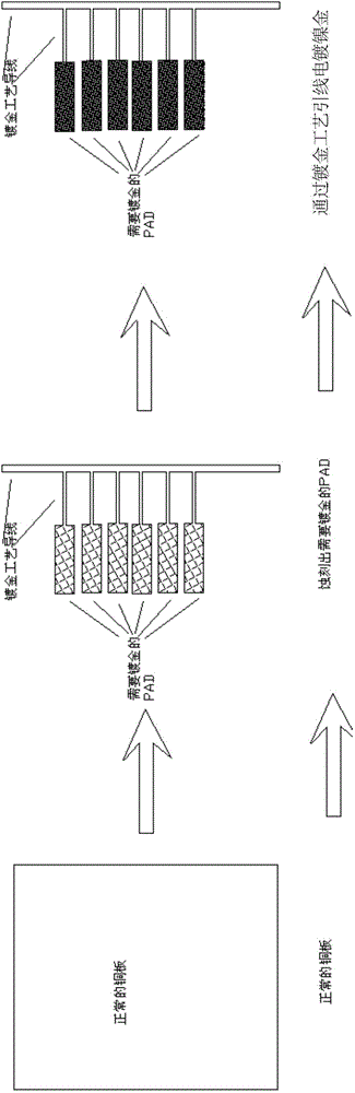
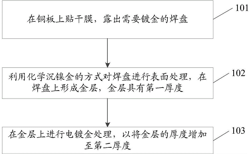
[0021] The embodiment of the present invention provides a circuit board and a gold-plating method thereof, which are used to solve the problems existing in the prior art that when the circuit board cannot pull the gold-plated process leads in the board, it is easy to cause a short circuit on the circuit board and low product yield when the circuit board is plated with gold. question.
[0022] The technical solution in the embodiment of the present application is to solve the above-mentioned technical problems, and the general idea is as follows:
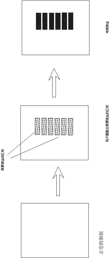
[0023] The gold plating method of the circuit board in an embodiment of the present invention comprises: pasting dry film on the copper plate, exposing the welding pad that needs gold plating; Utilizing the mode of electroless nickel-gold to carry out surface treatment to the welding pad, forming a gold layer on the welding pad , the gold layer has a first thickness; performing gold electroplating on the gold layer to increase the th...
PUM
| Property | Measurement | Unit |
|---|---|---|
| Thickness | aaaaa | aaaaa |
| Thickness | aaaaa | aaaaa |
Abstract
Description
Claims
Application Information