Method for electronic dynamic control of crystal silicon surface periodic micro-nano structures based on square hole assistance

A technology of electronic dynamic control and micro-nano structure, applied in the field of femtosecond laser applications, can solve the problems of inability to efficiently control the processing of surface periodic micro-nano structures, and achieve the improvement of processing accuracy and processing efficiency, reduction of energy consumption, and reduction of processing power. Effect

Active Publication Date: 2015-05-20
BEIJING INSTITUTE OF TECHNOLOGYGY
View PDF9 Cites 15 Cited by
  • Summary
  • Abstract
  • Description
  • Claims
  • Application Information

AI Technical Summary

Problems solved by technology

[0004] The purpose of the present invention is to solve the problem that the existing single mask can only realize one form of processing, and cannot realize the precise and efficient control processing of multiple forms of surfa

Method used


Image

  • Method for electronic dynamic control of crystal silicon surface periodic micro-nano structures based on square hole assistance

Examples


Embodiment approach

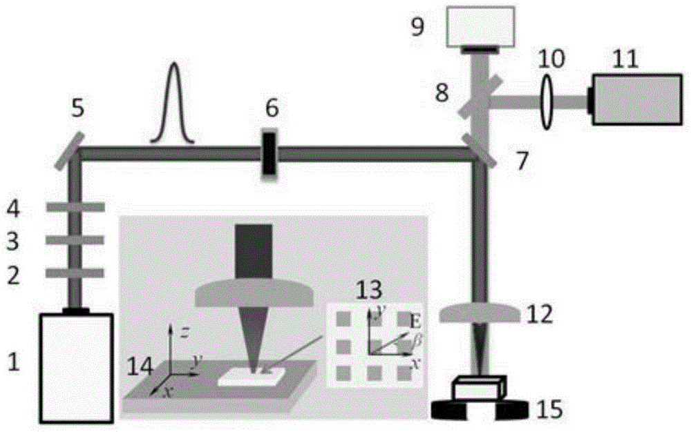
[0051] (1) Under a specific energy, by controlling the femtosecond laser direct writing speed and then adjusting the energy deposited on the surface of the material per unit area, the surface periodic micro-nano structure can be controlled. Specifically, the copper mesh with square holes is selected as a side length of 19 μm, and a 100mm plano-convex lens is used, at 0.1J / cm 2 Under the energy density of 1000Hz, the pulse repetition frequency is 1000Hz, the laser direct writing speed is increased from 100μm / s to 1000μm / s at intervals of 100, keeping the linear polarization direction parallel to the x-axis (one edge of the square hole), passing through the square hole The final focused femtosecond laser pulse regulates the excitation characteristics of the local instantaneous electronic dynamics in a specific area of ​​the irradiated area, so that the single crystal silicon can obtain different surface periodic micro-nano structures under the action of the direct writing femtose...


PUM


Abstract

The invention relates to a method for electronic dynamic control of crystal silicon surface periodic micro-nano structures based on square hole assistance and belongs to the technical field of femtosecond laser application. The method is based on local transient electronic excitation dynamic control, and femtosecond laser linear polarization is focused through an objective lens and then is focused on the surface of a material through a square hole copper wire mesh to achieve various precise control of different surface periodic micro-nano structures; by controlling laser scanning speed and pulse energy, ablation of strip-shaped surface corrugated structures and multi-point array micro-nano structures is achieved; by controlling the relative positions of the laser polarization direction and the direction (x axis) of the edge of a square hole, direction control of the periodic micro-nano structures can be achieved; by effectively adjusting the included angle between the linear polarization laser direction and the direction (x axis) of the edge of the square hole, selective ablation of the crystal silicon surface periodic micro-nano structures is achieved. Compared with existing methods, the method has the advantages that surface processing precision and efficiency are improved effectively, and efficient and accurate form control of the surface periodic micro-nano structures is achieved.

Description

technical field [0001] The invention relates to a method for generating periodic micro-nano structures on the surface of crystalline silicon, in particular to a method for generating micro-nano periodic structures on the surface of crystalline silicon regulated by femtosecond laser based on square-hole copper mesh-assisted electronic dynamic control, which belongs to femtosecond laser application technology field. Background technique [0002] The surface micro-nanostructure of solid materials is an important factor to control the optical, wettability, chemical, biological and other characteristics of the material surface. Therefore, effective adjustment and control of the micro-nanostructure of the solid material surface has become a research focus. With the emergence of mode-locking and amplification technology, femtosecond laser technology has developed rapidly. Femtosecond laser surface micro-nano processing has become a novel and effective surface treatment technology,...

Claims


Application Information

Patent Timeline
IPC IPC(8): B23K26/352B23K26/362B23K26/70
CPCB23K26/0643B23K26/354
Inventor 姜澜韩伟娜李晓炜
Owner BEIJING INSTITUTE OF TECHNOLOGYGY
Why Eureka
Try Eureka