Preparation method of heterojunction thermal photovoltaic cell

A thermal photovoltaic cell and heterojunction technology, which is applied in the manufacture of circuits, electrical components, and final products, can solve the problems of reducing the collection efficiency of photogenerated carriers, the number of semiconductor functional layers, and the impact on battery conversion efficiency. Conducive to battery efficiency, improved photoelectric conversion efficiency, and high photoelectric conversion efficiency

Active Publication Date: 2018-03-06
CHINA ELECTRONIC TECH GRP CORP NO 18 RES INST
View PDF4 Cites 1 Cited by
  • Summary
  • Abstract
  • Description
  • Claims
  • Application Information

AI Technical Summary

Problems solved by technology

Since the forbidden band width of the emission region on the incident light side of the cell is smaller than that of the base region, the collection efficiency of photogenerated carriers is reduced, which affects the improvement of the conversion efficiency of the cell, and the number of semiconductor functional layers is large, and the elements of each layer The composition is complex, the production is difficult, and the expensive GaSb and GaInAsSb materials are used, the cost of the battery is very high

Method used


Image

  • Preparation method of heterojunction thermal photovoltaic cell
  • Preparation method of heterojunction thermal photovoltaic cell

Examples


preparation example Construction

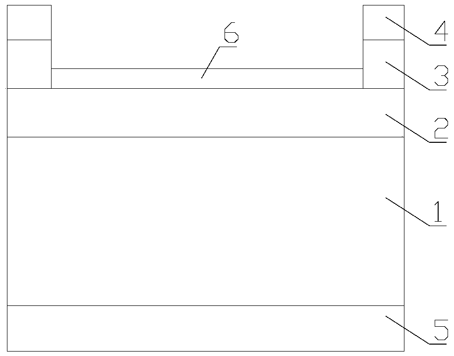
[0033] The method for preparing a heterojunction thermal photovoltaic cell is characterized in that it includes the following preparation steps:

[0034] Step 1: sequentially grow the emitter region, the electrode contact layer and the upper electrode on the base region

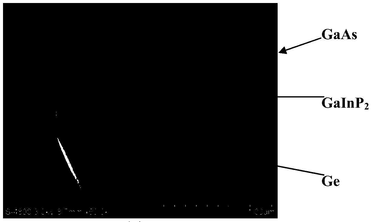
[0035] (1) Place the p-Ge layer substrate with a narrow bandgap width of 50-500 μm as the base area in the MOCVD equipment, and grow n-Ga with a thickness of less than 500 nm and a wider bandgap width on the p-Ge layer substrate x In y The p layer is used as an emission region, wherein x=0.4~0.8, y=1-x; the forbidden band width of the p-Ge layer is 0.66eV; the n-Ga x In y The band gap of the P layer is 1.9eV;

[0036] ⑵In n-Ga x In y The epitaxial growth of 30nm to 1000nm thick on the P layer is used as a heavily doped n-GaAs layer or a heavily doped n-GaInP layer for making an electrode contact layer;

[0037] (3) Evaporate a layer of Ag, Au, Cu, Ti, Pd, Ni or Al film on the electrode contact layer as th...

Embodiment

[0050] Step 1 Select the p-type Ge substrate as the base region

[0051] Doped with Be, Mg, B or Zn, the doping concentration is 10 15 ~10 17 cm -3 A p-type Ge single crystal with a relatively narrow band gap (about 0.66eV), cut along the Ge(001) crystal plane with an inclination of 6° in the [111] direction, and cut into a wafer substrate with a thickness of 50-500 μm as the base region 1;

[0052] Step 2 On the base region, grow the emitter region and the electrode contact layer with a wider band gap in sequence

[0053] Put the p-type Ge substrate in the MOCVD equipment, in GaInP 2 Before starting to grow, the p-Ge substrate was heated in H 2 Heating to 600-800°C in an atmosphere, maintaining the temperature and passing phosphine (PH 3 ) for 50 to 500 seconds, and then pass the carrier gas (H 2 ) carries the saturated vapor of the metal-organic source into the reaction chamber, the metal-organic source includes the precursors trimethylgallium (TMGa), trimethylindium (...


PUM

PropertyMeasurementUnit
thicknessaaaaaaaaaa
thicknessaaaaaaaaaa

Abstract

The invention relates to a method for manufacturing hetero-junction thermal photovoltaic batteries. The method includes manufacturing procedures of sequentially growing emitting regions, electrode contact layers and upper electrodes on the upper surfaces of base regions; photoetching the upper electrodes; eroding the upper electrodes and the electrode contact layers; manufacturing optical anti-reflection layers; arranging lower electrodes on the lower surfaces of the base regions by means of vapor deposition. The base regions comprise p-Ge layers with narrow forbidden bands. N-Ga<x>In<y>P layers with wide forbidden bands are used as the emitter regions, and the thicknesses of the n-Ga<x>In<y>P layers are smaller than 500nm. The method has the advantages that the n-Ga<x>In<y>P layers with the wide forbidden bands and precisely adjustable Ga to In proportions are used as the emitter regions, p-Ge substrates with narrow forbidden bands are used as the base regions, accordingly, hetero-junction structures with the emitter regions and the base regions which are provided with precisely matched crystal lattices can be formed, Ga<x>In<y>P / Ge interface recombination can be reduced, light absorbed by the emitter regions with wide band gaps can be reduced, light absorbed by the base regions can be increased, recombination of photon-generated carriers at the type-n emitter regions and the surfaces of the type-n emitter regions can be reduced, the photon-generated carrier collection efficiency can be improved, and the photoelectric conversion efficiency of the batteries can be effectively improved.

Description

technical field [0001] The invention belongs to the technical field of thermal photovoltaic cells, in particular to a method for preparing a heterojunction thermal photovoltaic cell. Background technique [0002] Thermal photovoltaic technology is a technology that directly converts the photon energy emitted by a heated high-temperature thermal radiator into electrical energy through a semiconductor p-n junction cell. The principle and concept of a complete thermo-photovoltaic system was proposed in the 1960s. Limited by the technological level at that time, it has been in the stage of theoretical research. In the early 1990s, gallium antimonide (GaSb) cells with low band gap were successfully prepared, and a series of thermal photovoltaic cells were successively developed. Its high efficiency, high stability, high weight specific power, and compatibility with combustion systems and isotope radiation systems The combination of advantages such as utilization has been verifie...

Claims


Application Information

Patent Timeline
Patent Type & Authority Patents(China)
IPC IPC(8): H01L31/18
CPCY02P70/50
Inventor 纪伟伟赵彦民方亮潘振赖运子乔在祥
Owner CHINA ELECTRONIC TECH GRP CORP NO 18 RES INST
Why Eureka
Try Eureka