Preparation method for photoelectric device

A technology for optoelectronic devices and light sources, applied in electrical components, semiconductor devices, circuits, etc., can solve problems affecting crystal growth quality, surface contamination, surface defects, etc., to improve free carrier concentration and mobility, and avoid surface defects. , the effect of improving the efficiency of the active area

Active Publication Date: 2015-05-20
TIANJIN SANAN OPTOELECTRONICS
View PDF4 Cites 17 Cited by
  • Summary
  • Abstract
  • Description
  • Claims
  • Application Information

AI Technical Summary

Problems solved by technology

Traditional epitaxial layer growth, due to many defects, affects the quality of crystal growth, affects carrier mobility, and then affects device performance. In addition, the substrate may cause surface contamination during the process of placing the substrate into the carrier tray and loading the reaction chamber. Surface defects will be caused after the growth of the epitaxial layer, therefore, it is necessary to invent a new epitaxial growth method to improve the above problems

Method used


Image

  • Preparation method for photoelectric device
  • Preparation method for photoelectric device

Examples


Embodiment 1

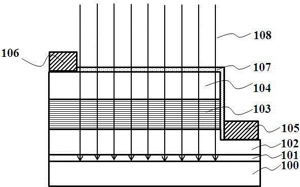
[0022] Such as figure 1 As shown, a schematic cross-sectional view of a preparation method of a light-emitting diode device, including the following steps:

[0023] (1) A substrate 100 is provided, and the substrate is selected from Al 2 o 3 , SiC, Si or GaN, Al is preferred in this embodiment 2 o 3 Substrate;

[0024] (2) After the substrate 100 is loaded into the reaction chamber and before growing the epitaxial layer, UV treatment is performed on the substrate. The UV light source is UVLED, and the UVLED treatment time is 0.1-10 min. The UVLED wavelength is 1-380nm. The light intensity is 0.1~1 000 000 mW / cm 2 ;

[0025] (3) Growing a buffer layer 101 on the UVLED-treated substrate 100, the buffer layer 101 is a gallium nitride (GaN) and / or aluminum nitride (AlN) layer or any combination thereof, with a thickness of 5-50 nm , UV treatment is carried out simultaneously during the growth process of the buffer layer 101, the UV light source is UVLED, the wavelength of U...

Embodiment 2

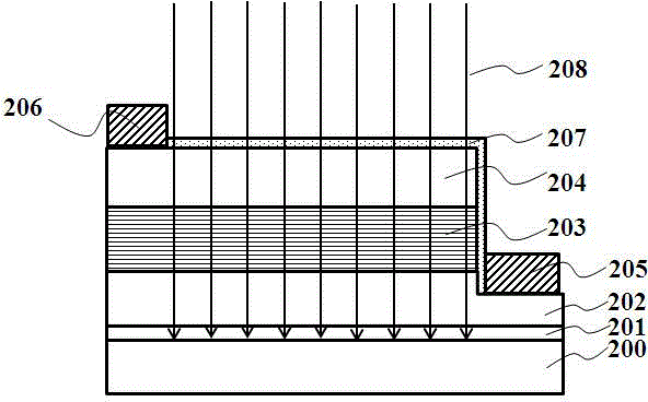
[0032] Such as figure 2 As shown, a schematic cross-sectional view of a preparation method of a solar cell device, comprising the following steps:

[0033] (1) A substrate 200 is provided, and the substrate is selected from Al 2 o 3 , SiC, Si or GaN, Al is preferred in this embodiment 2 o 3 Substrate;

[0034] (2) After the substrate 200 is loaded into the reaction chamber and before growing the epitaxial layer, UV treatment is performed on the substrate, the UV treatment time is 0.1-10 min, the UV light source is UVLED, and the UVLED wavelength is 1-380 nm, The light intensity of UV LED is 0.1~1 000 000 mW / cm 2 ;

[0035](3) Growing a buffer layer 201 on the UVLED-treated substrate 200, the buffer layer 201 is a gallium nitride (GaN) and / or aluminum nitride (AlN) layer or any combination thereof, with a thickness of 5-50 nm , UV treatment is carried out simultaneously during the growth process of the buffer layer 201, the UV light source is UVLED, the wavelength of UV...


PUM


Abstract

The invention discloses a preparation method for a photoelectric device. The preparation method comprises the following steps: performing UVLED (ultraviolet light-emitting diode) processing on a substrate after loading the substrate into a reaction chamber and before growing an epitaxial layer, thereby effectively reducing surface organic or / and inorganic substance pollution caused by processes of putting the substrate into a slide glass plate and loading the substrate into the reaction chamber, enabling the surface to be clean before growing the epitaxial layer and avoiding surface defects after growing the epitaxial layer; growing N-type, active and P-type epitaxial layers on the substrate subjected to the UVLED processing and performing UVLED processing in each epitaxial layer growing process, thereby effectively reducing point defects in each of doped or non-doped AlInGaN, AlGaInP, AlGaInAs multi-element epitaxial layers, improving the crystal quality and breaking Mg-H passivated bonds of the P-type layer. Therefore, free carrier concentration and migration rate of the N-type and P-type layers can be effectively increased, the active region efficiency is improved, and the performances of the photoelectric device is improved. The preparation method is suitable for a semiconductor photoelectric device.

Description

technical field [0001] The invention belongs to the technical field of semiconductor optoelectronics, and in particular relates to a preparation method of an optoelectronic device. Background technique [0002] With the increasing application of semiconductor optoelectronic devices (such as light-emitting diodes and solar cells), further improving their optoelectronic performance has become the research focus of the industry. Traditional epitaxial layer growth, due to many defects, affects the quality of crystal growth, affects carrier mobility, and then affects device performance. In addition, the substrate may cause surface contamination during the process of placing the substrate into the carrier tray and loading the reaction chamber. Surface defects will be caused after the growth of the epitaxial layer, therefore, it is necessary to invent a new epitaxial growth method to improve the above problems. Contents of the invention [0003] In view of the above problems, th...

Claims


Application Information

Patent Timeline
Patent Type & Authority Applications(China)
IPC IPC(8): H01L33/00H01L31/18
CPCH01L31/18H01L31/1876H01L33/005Y02P70/50
Inventor 董木森申利莹王良均吴超瑜王笃祥
Owner TIANJIN SANAN OPTOELECTRONICS
Why Eureka
Try Eureka