A kind of preparation method of intermetallic compound film

A technology of intermetallic compounds and films, applied in electrolytic coatings, surface reaction electrolytic coatings, coatings, etc., can solve problems such as high cost, high energy consumption, and slow film growth rate, and achieve accelerated growth rate and fast growth rate , Improve the effect of mechanical properties

Active Publication Date: 2018-01-16
DALIAN UNIV OF TECH
View PDF8 Cites 0 Cited by
  • Summary
  • Abstract
  • Description
  • Claims
  • Application Information

AI Technical Summary

Problems solved by technology

However, the above method has the following disadvantages: it needs to be prepared in a high temperature environment; it needs to be prepared in a vacuum environment, which has a strong dependence on equipment; it consumes a lot of energy and costs high; the film growth rate is slow

Method used


Image

  • A kind of preparation method of intermetallic compound film
  • A kind of preparation method of intermetallic compound film
  • A kind of preparation method of intermetallic compound film

Examples


Embodiment 1

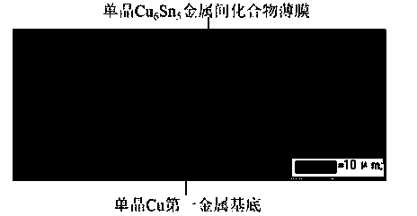
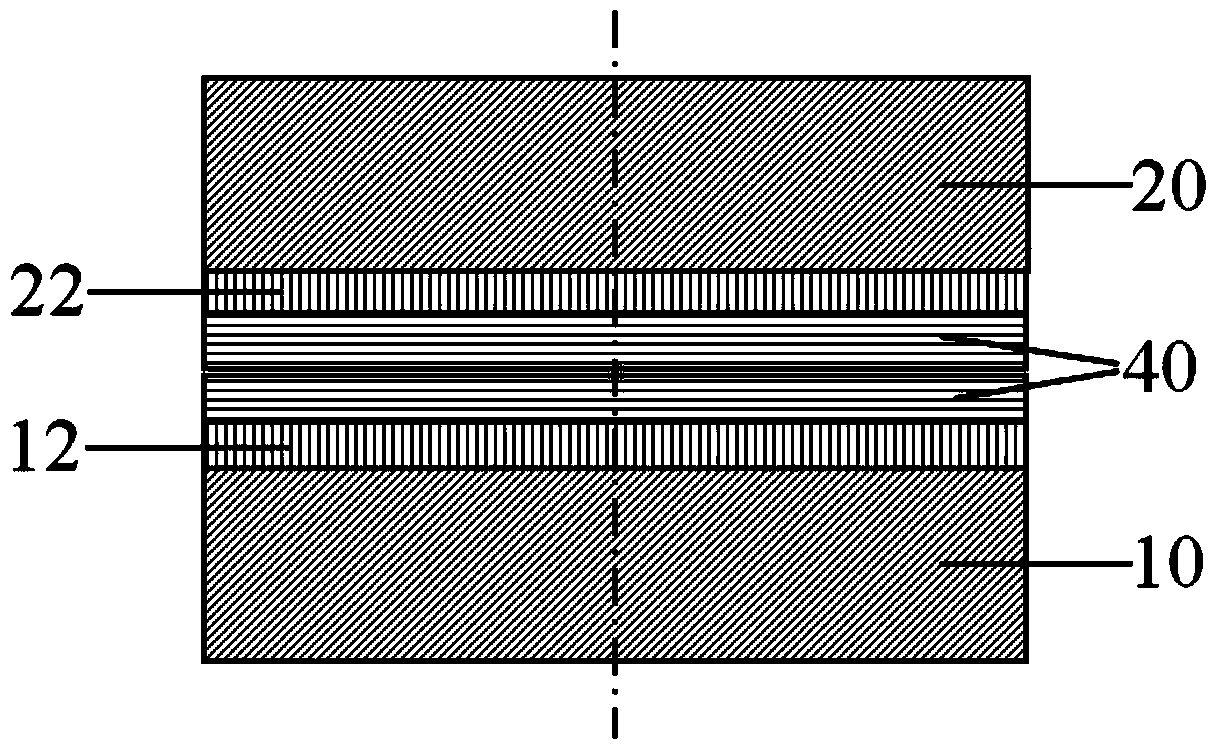
[0046] Such as figure 1 , figure 2 with Figure 5 Shown, the preparation method of intermetallic compound thin film of the present invention can be realized by following specific processing steps:

[0047] Step 1: providing a first metal substrate of single crystal Cu, sputtering a first solder metal layer of Sn with a thickness of 0.25 μm on the first metal substrate of single crystal Cu; providing a second metal substrate of polycrystalline Cu, on the first metal substrate of polycrystalline Cu Sputtering a 0.25 μm thick Sn second solder metal layer on the crystal Cu second metal substrate;

[0048] Step 2: coating flux on the surfaces of the first Sn solder metal layer and the Sn second solder metal layer;

[0049] Step 3: Aligning the first Sn solder metal layer and the Sn second solder metal layer, and placing them in contact to form an assembly;

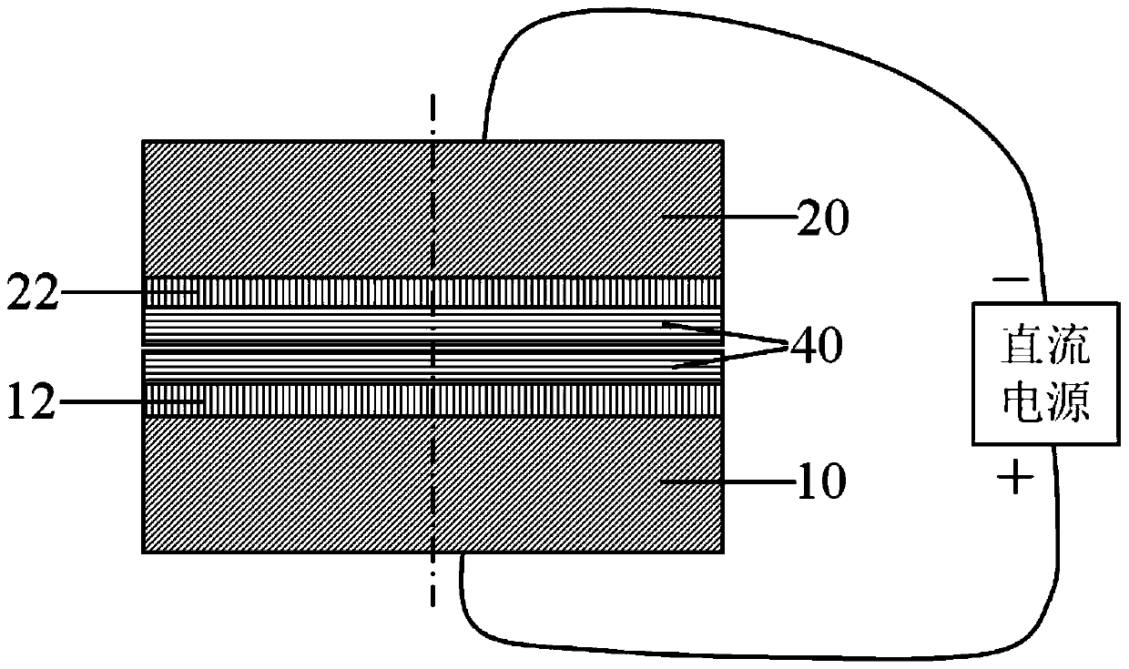
[0050] Step 4: Heating the assembly formed in Step 3 to 260°C for brazing reflow, while applying a certain DC current so...

Embodiment 2

[0054] Such as image 3 , Figure 4 with Figure 5 Shown, the preparation method of intermetallic compound thin film of the present invention can be realized by following specific processing steps:

[0055] Step 1: providing a polycrystalline Ni first metal substrate, vapor-depositing a 0.5 μm thick Sn first solder metal layer on the polycrystalline Ni first metal substrate; providing a polycrystalline Ni second metal substrate;

[0056] Step 2: coating flux on the surface of the Sn first solder metal layer and the polycrystalline Ni second metal substrate;

[0057] Step 3: aligning the first Sn solder metal layer and the second polycrystalline Ni metal substrate, and placing them in contact to form an assembly;

[0058] Step 4: Heating the assembly formed in Step 3 to 260°C for brazing reflow, while applying a certain DC current so that the current density passing through the polycrystalline Ni first metal substrate is 0.75×10 4 A / cm 2 , and the current direction is dire...

Embodiment 3

[0061] Such as figure 1 , figure 2 with Figure 5 Shown, the preparation method of intermetallic compound thin film of the present invention can be realized by following specific processing steps:

[0062] Step 1: Provide a single crystal Cu first metal substrate, electroplate a 10 μm thick Sn-Cu first solder metal layer on the single crystal Cu first metal substrate; provide a polycrystalline Cu second metal substrate, and Electroplating a 10 μm thick Sn-Cu second solder metal layer on the Cu second metal substrate;

[0063] Step 2: Coating flux on the surfaces of the first Sn-Cu solder metal layer and the Sn-Cu second solder metal layer;

[0064] Step 3: aligning the Sn-Cu first solder metal layer and the Sn-Cu second solder metal layer, and placing them in contact to form an assembly;

[0065] Step 4: Perform brazing reflow on the assembly formed in Step 3 at 260°C, and apply a certain DC current at the same time, so that the current density passing through the first m...


PUM

PropertyMeasurementUnit
thicknessaaaaaaaaaa

Abstract

A preparation method of an intermetallic compound thin film is to prepare a first solder metal layer on a first metal base, a second solder metal layer can be prepared on a second metal base, and then the first solder coated with flux The metal layer and the second solder metal layer are placed in alignment and contact to form an assembly; or the first solder metal layer and the second metal base coated with flux are placed in alignment to form an assembly; the assembly is heated to the Brazing reflow is carried out at the required temperature, and a direct current with a current density of I / S is applied at the same time, until the brazing metal layer is melted and the brazing reaction is completely transformed into an intermetallic compound, and the residual second metal substrate is removed to obtain an intermetallic compound film. The invention applies a direct current to form a current density during brazing reflow, which accelerates the formation rate of the intermetallic compound, and the formed intermetallic compound can be single crystal or have a single orientation; realizes the low-temperature preparation of the intermetallic compound film, and the film has a dense surface Smooth, good film quality.

Description

technical field [0001] The invention belongs to the field of functional materials and relates to a preparation method of an intermetallic compound thin film. Background technique [0002] Intermetallic compounds have diverse bonding types (metallic bonds and covalent bonds), special crystal structures, electronic structures, and energy band structures, and thus have many special physical, chemical and mechanical properties. For example, unique electrical properties, magnetic properties, optical properties, acoustic properties, electron emission properties, catalytic properties, oxidation resistance and corrosion resistance. Intermetallic compounds can not only be used as high-temperature structural materials, but also have a very wide range of applications in the field of functional materials, such as semiconductor materials, magnetic materials, memory alloys, hydrogen storage materials, high-brightness electron source materials, and catalysts. However, due to the brittlene...

Claims


Application Information

Patent Timeline
Patent Type & Authority Patents(China)
IPC IPC(8): C25D11/00
Inventor 黄明亮赵宁张志杰杨帆黄斐斐马海涛赵杰
Owner DALIAN UNIV OF TECH
Why Eureka
Try Eureka